

STS25NH3LL
N-CHANNEL 30V - 0.0032 Ω - 25A SO-8
STripFET™ III MOSFET FOR DC-DC CONVERSION
TYPE
V
DSS
STS25NH3LL 30 V <0.0035
■ TYPICAL R
■ OPTIMAL R
■ CONDUCTION LOSSES REDUCED
■ SWITCHING LOSSES REDUCED
(on) = 0.0032 Ω @ 10V
DS
(on) x Qg TRADE-OFF @ 4.5V
DS
R
DS(on)
I
D
25 A
Ω
DESCRIPTION
The STS25NH3LL utilizes the latest advanced design
rules of ST's propetary STripFET™ technology. This
novel 0.6µ process coupled to unique metalization
techniques re alizes the most advanced low voltage
MOSFET in SO- 8 eve r pro duced . It is there fore s uit ab le
for the most demanding DC-DC converter applications
where high efficiency is to be achived at high output
current.
APPLICATIONS
■ DC-DC CONVERTERS FOR TELECOM AND
NOTEBOOK CPU CORE
■ SYNCHRONOUS RECTIFIER
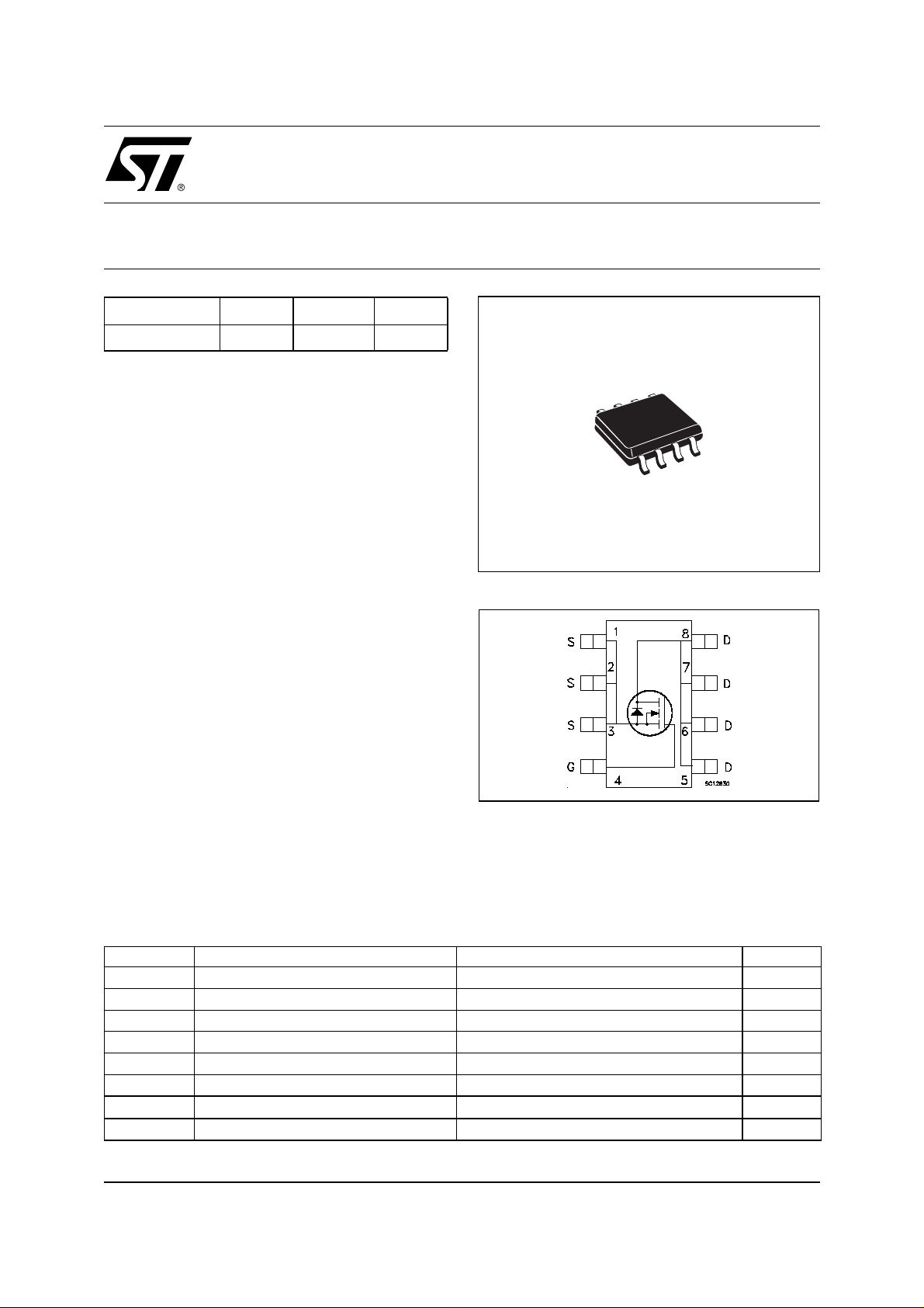
SO-8
INTERNAL SCHEMATIC DIAGRAM
ABSOLUTE MAXIMUM RATINGS
Symbol Parameter Value Unit
V
DS
V
DGR
V
GS
I
D
I
D
(
I
DM
E
AS
P
tot
(
Pulse widt h l i m i ted by safe operating area.
•)
.
Drain-source Voltage (VGS = 0)
Drain-gate Voltage (RGS = 20 kΩ)
30 V
30 V
Gate- source Voltage ± 18 V
Drain Current (continuous) at TC = 25°C
Drain Current (continuous) at TC = 100°C
•)
Drain Current (pulsed) 100 A
(1)
Single Pulse Avalanche Energy 200 mJ
Total Dissipation at TC = 25°C
(1)
Starting Tj = 25 oC ID = 12.5A VDD = 30V
25 A
18 A
3.2 W
1/8September 2003
STS25NH3LL
THERMA L D ATA
Rthj-amb
Rthj-lead
T
T
stg
(*)
When Mounted on 1 inch2 FR-4 board, 2 oz of Cu and t [ 10 sec.
(*)
Thermal Resistance Junction-ambient
Thermal Resistance Junction-leads
Maximum Operating Junction Temperature
j
Storage Temperature
Max
Max
47
16
-55 to 175
-55 to 175
°C/W
°C/W
°C
°C
ELECTRICAL CHARACTERISTICS (T
= 25 °C unless otherwise specified)
case
OFF
Symbol Parameter Test Conditions Min. Typ. Max. Unit
I
= 250 µA, VGS = 0
D
V
= Max Rating
DS
V
= Max Rating TC = 125°C
DS
V
= ± 18 V
GS
30 V
1
10
±100 nA
ON
V
(BR)DSS
I
DSS
I
GSS
(*)
Drain-source
Breakdown Voltage
Zero Gate Voltage
Drain Current (V
GS
Gate-body Leakage
Current (V
DS
= 0)
= 0)
Symbol Parameter Test Conditions Min. Typ. Max. Unit
V
V
GS(th)
R
DS(on)
Gate Threshold Voltage
Static Drain-source On
Resistance
= VGS I
DS
= 10 V ID = 12.5 A
V
GS
V
= 4.5 V ID = 12.5 A
GS
= 250 µA
D
1V
0.0032
0.004
0.0035
0.005
DYNAMIC
Symbol Parameter Test Conditions Min. Typ. Max. Unit
(*)
g
fs
C
iss
C
oss
C
rss
Forward Transconductance
Input Capacitance
Output Capacitance
Reverse Transfer
Capacitance
V
= 10 V ID= 12.5 A
DS
= 25V, f = 1 MHz, VGS = 0
V
DS
30 S
4450
655
50
µA
µA
Ω
Ω
pF
pF
pF
2/8

STS25NH3LL
ELECTRICAL CHARACTERISTICS (continued)
SWITCHING ON
Symbol Parameter Test Conditions Min. Typ. Max. Unit
= 15 V ID = 12.5 A
t
d(on)
Turn-on Delay Time
t
r
Rise Time
V
DD
R
= 4.7 Ω VGS = 10 V
G
(Resistive Load, Figure 1)
Q
g
Q
gs
Q
gd
Total Gate Charge
Gate-Source Charge
Gate-Drain Charge
=15V ID=25A VGS=4.5 V
V
DD
(see test circuit, Figure 2)
SWITCHING OFF
Symbol Parameter Test Conditions Min. Typ. Max. Unit
= 15 V ID = 12.5 A
t
d(off)
Turn-off Delay Time
t
f
Fall Time
V
DD
R
= 4.7Ω, V
G
GS
= 10 V
(Resistive Load, Figure 3)
SOURCE DRAIN DIODE
Symbol Parameter Test Conditions Min. Typ. Max. Unit
I
SD
I
SDM
V
SD
t
rr
Q
rr
I
RRM
(*)
Pulsed: P ul se duration = 300 µs, duty cycle 1.5 %.
(
•)Pulse width limited by s afe operating area.
Source-drain Current
Source-drain Current (pulsed)
(*)
Forward On Voltage
Reverse Recovery Time
Reverse Recovery Charge
Reverse Recovery Current
I
= 25 A VGS = 0
SD
= 25 A di/dt = 100A/µs
I
SD
V
= 25 V Tj = 150°C
DD
(see test circuit, Figure 3)
18
50
30
12.5
10
75
8
32
34
2.1
40 nC
25
100
1.2 V
ns
ns
nC
nC
ns
ns
A
A
ns
nC
A
Safe Operating Area
Thermal Impedance
3/8
 Loading...