

SGS Thomson Microelectronics STS12NF30L Datasheet
STS12NF30L
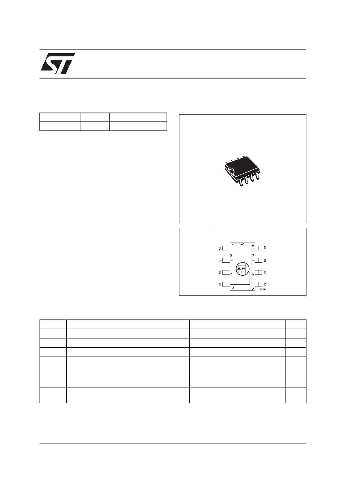
N - CHANNEL 30V - 0.0085Ω - 12A SO-8
STripFET POWER MOSFET
TYPE V
ST S12NF30L 30 V < 0 . 01 Ω 12 A
■ TYPICALR
■ STANDARD OUTLINEFOR EASY
DS(on)
DSS
= 0.0085 Ω
R
DS(on)
I
D
AUTOMATEDSURFACEMOUNTASSEMBLY
■ LOW THRESHOLDDRIVE
DESCRIPTION
This Power MOSFET is the second generation of
STMicroelectronics unique ” Single Feature
Size
”
strip-based process. The resulting
transistor shows extremely high packing density
for low on-resistance, rugged avalanche
characteristics and less critical alignment steps
therefore a remarkable manufacturing
reproducibility.
APPLICATIONS
■ DC MOTOR DRIVE
■ DC-DCCONVERTERS
■ BATTERYMANAGMENTIN NOMADIC
EQUIPMENT
■ POWERMANAGEMENT IN
PORTABLE/DESKTOPPC
s
SO-8
INTERNAL SCHEMATIC DIAGRAM
ABSOLUTE MAXIMUM RATINGS
Symb o l Parameter Value Unit
V
V
V
I
DM
P
(•) Pulse width limited by safeoperating area
May 1999
Drain-source Voltage (VGS=0) 30 V
DS
Drain- gat e Voltage (RGS=20kΩ)30V
DGR
Gate-s ource Voltage ± 20 V
GS
Drain Current (co nt inu ous ) at Tc = 25oC
I
D
Drain Current (co nt inu ous ) at T
(•) Drain Current (pulsed) 48 A
Tot al Dissipat ion at Tc=25oC 2.5 W
tot
=100oC
c
12
7.5
A
A
1/8
STS12NF30L
THERMAL DATA
R
thj-amb
T
Tj
(*)T hermal R es istance Junction-am bie nt
Maximum O perating Juncti on Temperat ur e
stg
St orage Tempe ra tur e
50
150
-55 to 150
o
C/W
o
o
C
C
(*)
Mountedon FR-4board (t
ELECTRICAL CHARACTERISTICS (T
≤ 10
sec)
=25oC unless otherwisespecified)
case
OFF
Symbol Parameter Test Conditions Min. Typ. Max. Unit
V
(BR)DSS
Drain-source
ID=250µAVGS=0 30 V
Break dow n Volt age
I
DSS
I
GSS
Zero Gate Voltage
Drain Current (V
GS
Gat e- bod y Leakage
Current (V
DS
=0)
=0)
V
=MaxRating
DS
=MaxRating Tc=125oC
V
DS
V
=± 20 V
GS
1
10
100 nA
±
ON (∗)
Symbol Parameter Test Conditions Min. Typ. Max. Unit
V
GS(th)
R
DS(on)
I
D(on)
Gate Threshold Voltage VDS=VGSID= 250µA11.62.5V
Sta t ic Drain-sour c e On
Resistance
VGS=10V ID=6A
=4.5V ID=6A
V
GS
On State Drain Current VDS>I
D(on)xRDS(on )max
0.0085
0.01
12 A
0.01
0.012ΩΩ
VGS=10V
DYNAMIC
µA
µA
Symbol Parameter Test Conditions Min. Typ. Max. Unit
g
(∗)Forward
fs
VDS>I
D(on)xRDS(on )maxID
=6A 20 S
Tr ansc on duc tance
C
C
C
Input Capacit ance
iss
Out put Capacitance
oss
Reverse Transfer
rss
VDS=25V f=1MHz VGS= 0 V 2400
590
200
Capacit a nc e
2/8
pF
pF
pF
STS12NF30L
ELECTRICAL CHARACTERISTICS
(continued)
SWITCHING ON
Symbol Parameter Test Conditions Min. Typ. Max. Unit
t
d(on)
Tur n-on Delay Time
Rise Time
t
r
VDD=15V ID=6A
R
=4.7
G
Ω
VGS=4.5V
35
90
(Resis t iv e Load, see f ig. 3 )
Q
Q
Q
Tot al Gate Char ge
g
Gat e- Source Charge
gs
Gate-Drain Charge
gd
VDD=24V ID=12A VGS=4.5V 35
9
18
50 nC
SWITCHING OFF
Symbol Parameter Test Conditions Min. Typ. Max. Unit
t
d(off)
Tur n-of f Delay Time
t
Fall T ime
f
VDD=15V ID=6A
=4.7 Ω VGS=4.5V
R
G
90
45
(Resis t iv e Load, see f ig. 3 )
t
r(Voff)
t
t
Off-volt age Rise Time
Fall T ime
f
Cross-over Time
c
V
=24V ID=12A
clamp
=4.7 Ω VGS=4.5V
R
G
(Indu ct iv e Load, see fig . 5)
35
35
80
SOURCEDRAINDIODE
Symbol Parameter Test Conditions Min. Typ. Max. Unit
I
V
I
SDM
SD
Q
I
RRM
SD
t
Source-drain Current
(•)
Source-drain Current
12
48
(pulsed)
(∗)ForwardOnVoltage ISD=12A VGS=0 1.2 V
Reverse Recovery
rr
Time
Reverse Recovery
rr
ISD= 12 A di/dt = 100 A /µs
=15V Tj=150oC
V
DD
(see test circuit, fig. 5)
45
70
Charge
Reverse Recovery
3
Current
ns
ns
nC
nC
ns
ns
ns
ns
ns
A
A
ns
nC
A
(∗) Pulsed:Pulse duration = 300 µs, duty cycle 1.5%
(•) Pulse width limited by safe operating area
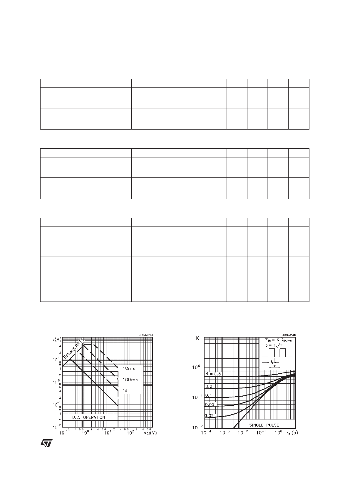
SafeOperating Area ThermalImpedance
3/8
 Loading...