

1/11June 2003
STD2NC45-1
STQ1NC45
N-CHANNEL 450V - 4.1Ω - 1 .5 A IPAK / TO-92
SuperMESH™Power MOSFET
■ TYPICAL R
DS
(on) = 4.1 Ω
■ EXTREMELY HIGHdv/dt CAPABILITY
■ 100% AVALANCHE TESTED
■ GATE CHARGE MINIMIZED
■ NEW HIGH VOLTAGE BENCHMARK
DESCRIPTION
The SuperMESH™ series is obtained through an
extreme optimization of ST’s we ll established stripbased PowerMESH™ layout. In addition to pushing
on-resistance significantly down, special careis taken to ensure a very good dv/dt capability for the
most demanding applications. Such series complements ST full range of high voltage MOSFETs including revolutionary MDm es h™ products.
APPLICATIONS
■ SWITCH MODE LOW POWER SUPPLIES
(SMPS)
■ LOW POWER, LOW COST CFL (COMPACT
FLUORESCENT LAMPS)
■ LOW POWER BATTERY CHARGERS
ORDERING INFORMATION
TYPE V
DSS
R
DS(on)
I
D
Pw
STD2NC45-1
STQ1NC45
450 V
450 V
< 4.5 Ω
< 4.5 Ω
1.5 A
0.5 A
30 W
3.1 W
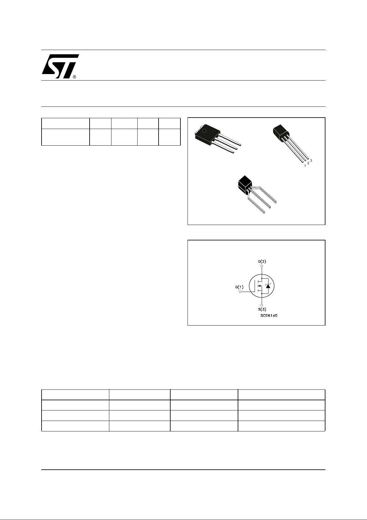
SALES TYPE MARKING PACKAGE PACKAGING
STD2NC45-1 D2NC45 IPAK TUBE
STQ1NC45 Q1NC45 TO-92 BULK
STQ1NC45-AP Q1NC45 TO-92 AMMOPAK
IPAK
3
2
1
TO-92
TO-92 (Ammopack)
INTERNAL SCHEMATIC DIAGRAM
STD2NC45-1, STQ1NC45
2/11
ABSOLUTE MAXIMUM RATINGS
() Pulse width limited by safe operating area
(1) I
SD
≤0.5A, di/dt ≤100A/µs, VDD≤ V
(BR)DSS,Tj≤TJMAX.
THERMAL DATA
AVALANCHE CHARACTERISTICS
Symbol Parameter Value Unit
STD2NC45-1 STQ1NC45
V
DS
Drain-source Voltage (VGS=0)
450 V
V
DGR
Drain-gate Voltage (RGS=20kΩ)
450 V
V
GS
Gate- source Voltage ± 30 V
I
D
Drain Current (continuos) at TC= 25°C
1.5 0.5 A
I
D
Drain Current (continuos) at TC= 100°C
0.95 0.315 A
IDM()
Drain Current (pulsed) 6 2 A
P
TOT
Total Dissipation at TC= 25°C
30 3.1 W
Derating Factor 0.24 0.025 W/°C
dv/dt (1) Peak Diode Recovery voltage slope 3 V/ns
T
j
T
stg
Operating Junction Temperature
Storage Temperature
-65 to 150
-65 to 150
°C
°C
IPAK TO-92
Rthj-case Thermal Resistance Junction-case Max 4.1 °C/W
Rthj-amb Thermal Resistance Junction-ambient Max 100 120 °C/W
Rthj-lead Thermal Resistance Junction-lead Max 40 °C/W
T
l
Maximum Lead Temperature For Soldering
Purpose
275 260 °C
Symbol Parameter Max Value Unit
IPAK TO-92
I
AR
Avalanche Current, Repetitive or Not-Repetitive
(pulse width limited by T
j
max)
1.5 A
E
AS
Single Pulse Avalanche Energy
(starting T
j
= 25 °C, ID=IAR,VDD=50V)
25 mJ
3/11
STD2NC45-1, STQ1NC45
ELECTRICAL CHARACTERISTICS (TCASE =25°C UNLESS OT HERWISE SPECIFIED)
ON/OFF
DYNAMIC
SWITCHING ON
SWITCHING OFF
SOURCE DRAIN DIODE
Note: 1. Pulsed: Pulse duration = 300 µs, duty cycle 1.5 %.
2. Pulse width limited by safe operating area.
Symbol Parameter Test Conditions Min. Typ. Max. Unit
V
(BR)DSS
Drain-source
Breakdown Voltage
ID= 250 µA, VGS= 0 450 V
I
DSS
Zero Gate Voltage
Drain Current (V
GS
=0)
V
DS
= Max Rating
VDS= Max Rating, TC= 125 °C
1
50
µA
µA
I
GSS
Gate-body Leakage
Current (V
DS
=0)
V
GS
= ± 30V ±100 nA
V
GS(th)
Gate Threshold Voltage
V
DS=VGS,ID
= 250µA
2.3 3 3.7 V
R
DS(on)
Static Drain-source On
Resistance
VGS=10V,ID= 0.5 A 4.1 4.5 Ω
Symbol Parameter Test Conditions Min. Typ. Max. Unit
g
fs
(1) Forward Transconductance VDS>I
D(on)xRDS(on)max,
ID= 0.5 A
1.1 S
C
iss
C
oss
C
rss
Input Capacitance
Output Capacitance
Reverse Transfer
Capacitance
V
DS
=25V,f=1MHz,VGS=0
160
27.5
4.7
pF
pF
pF
Symbol Parameter Test Conditions Min. Typ. Max. Unit
t
d(on)
t
r
Turn-on Delay Time
Rise Time
VDD=225V,ID= 0.5 A
R
G
= 4.7Ω VGS=10V
(Resistive Load see, Figure 3)
6.7
4
ns
ns
Q
g
Q
gs
Q
gd
Total Gate Charge
Gate-Source Charge
Gate-Drain Charge
V
DD
=360V,ID= 1.5 A,
VGS=10V,RG= 4.7Ω
7
1.3
3.2
10
nC
nC
nC
Symbol Parameter Test Conditions Min. Typ. Max. Unit
t
r(Voff)
t
f
t
c
Off-voltage Rise Time
Fall Time
Cross-over Time
V
DD
= 360V, ID= 1.5 A,
R
G
=4.7Ω, VGS= 10V
(Inductive Load see, Figure 5)
8.5
12
18
ns
ns
ns
Symbol Parameter Test Conditions Min. Typ. Max. Unit
I
SD
I
SDM
(2)
Source-drain Current
Source-drain Current (pulsed)
1.5
6.0
A
A
V
SD
(1)
Forward On Voltage
ISD= 1.5 A, VGS=0
1.6 V
t
rr
Q
rr
I
RRM
Reverse Recovery Time
Reverse Recovery Charge
Reverse Recovery Current
I
SD
= 1.5 A, di/dt = 100A/µs
VDD=100V,Tj=150°C
(see test circuit, Figure 5)
225
530
4.7
ns
µC
A
STD2NC45-1, STQ1NC45
4/11
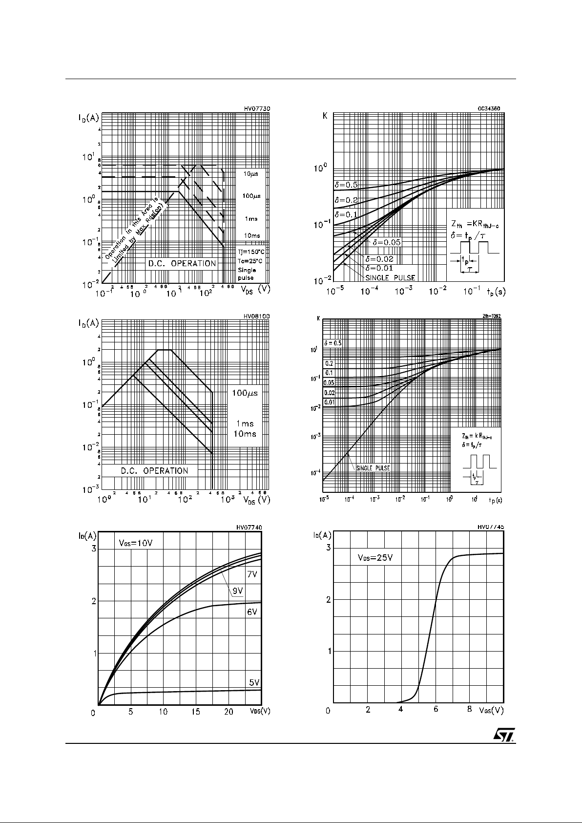
Safe Operating Area For IPAK
Thermal Impedance For TO-92Safe Operating Area For TO-92
Thermal Imped ance For IPAK
Output Characteristics
Transfer Characteristics

5/11
STD2NC45-1, STQ1NC45
Normalized Gate Threshold Voltage v s Temp. Normalized On Resi stance vs Temper ature
Gate Charge vs Gate-so urce V oltage
Transconductance Static Drain-source On Resistance
Capacitance Variations

STD2NC45-1, STQ1NC45
6/11
Maximum Avalanche Energy vs Temperature
Max Id Current vs Tc
Source-drain Diode Forward Characteristics
Normalized BVDSS vs Temperature

7/11
STD2NC45-1, STQ1NC45
Fig. 5: Test Circuit For Induct ive Load Switching
And Diode Recovery Times
Fig. 4: Gate Charge tes t Circuit
Fig. 2: Unclamped Inductive WaveformFig. 1: Unclamped Inductive Load Test Circuit
Fig. 3: Switching Times Test Circuit For
Resistive Load

STD2NC45-1, STQ1NC45
8/11
DIM.
mm inch
MIN. TYP. MAX. MIN. TYP. MAX.
A 2.2 2.4 0.086 0.094
A1 0.9 1.1 0.035 0.043
A3 0.7 1.3 0.027 0.051
B 0.64 0.9 0.025 0.031
B2 5.2 5.4 0.204 0.212
B3 0.85 0.033
B5 0.3 0.012
B6 0.95 0.037
C 0.45 0.6 0.017 0.023
C2 0.48 0.6 0.019 0.023
D 6 6.2 0.236 0.244
E 6.4 6.6 0.252 0.260
G 4.4 4.6 0.173 0.181
H 15.9 16.3 0.626 0.641
L 9 9.4 0.354 0.370
L1 0.8 1.2 0.031 0.047
L2 0.8 1 0.031 0.039
A
C2
C
A3
H
A1
D
L
L2
L1
1 3
= =
B3
B
B6
B2
E
G
= =
= =
B5
2
TO-251 (IPAK) MECHANI CAL DAT A
0068771-E

9/11
STD2NC45-1, STQ1NC45
DIM.
mm. inch
MIN. TYP MAX. MIN. TYP. MAX.
A 4.32 4.95 0.170 0.194
b 0.36 0.51 0.014 0.020
D 4.45 4.95 0.175 0.194
E 3.30 3.94 0.130 0.155
e 2.41 2.67 0.094 0.105
e1 1.14 1.40 0.044 0.055
L 12.70 15.49 0.50 0.610
R 2.16 2.41 0.085 0.094
S1 0.92 1.52 0.036 0.060
W 0.41 0.56 0.016 0.022
V5° 5°
TO-92 MECHANICAL DATA

STD2NC45-1, STQ1NC45
10/11

11/11
STD2NC45-1, STQ1NC45
Information furnished is believed to be accurate and reliable. However, STMicroelectronics assumes no responsibility for the consequences
of use of such informa tion n or for an y infring ement of patent s or other rig hts of third part ies which may resu lt from its use . No l i cen se i s
granted by implication or otherwise under any patent or patent rights of STMicroelectronics. Specification mentioned in this publication are
subject to change without notice. This publication supersedes and replaces all information previously supplied. STMicroelectronics products
are not authorized for use as critical compo nents in life support devices or systems without express written approval of STMicroelectronics.
The ST logo is a trademark of STMicroelectronics
© 2000 STMicroelectronics – Printed in Italy – All Rights Reserved
STMicroelectronics GROUP OF COMPANIES
Australia - Brazil - China - Finland - France - Germany - Hong Kong - India - Italy - Japan - Malaysia - Malta - Morocco -
Singapore - Spain - Sweden - Switzerland - United Kingdom - U.S.A.
http://www.st.com
 Loading...