

SGS Thomson Microelectronics STQ1HNC60 Datasheet
STQ1HNC60
N-CHANNEL 600V - 7Ω - 0.4A TO-92
PowerMesh™II MOSFET
PRELIMINARY DATA
TYPE V
DSS
R
DS(on)
I
D
STQ1HNC60 600 V < 8 Ω 0.4 A
■ TYPICAL R
■ EXTREMELY HIGH dv /d t C APABILITY
■ 100% AVALANCHE TESTED
■ NEW HIGH VOLTAGE BENCHMARK
■ GATE CHARGE MINIMIZED
(on) = 7 Ω
DS
DESCRIPTION
Using the latest high voltage MESH OVERLAY™II
process, STMicroelectronics has designed an advanced family of power MOSFETs with outstanding
performances. The new patent pending strip layout
coupled with the Company’s proprietary edge termination structure, gives the lowest RDS(on) per area,
exceptional avalanche and dv/dt capabilities and
unrivalled gate charge and switching characteristics.
APPLICATIONS
■ SWITCH MODE LOW POWER SUPPIES
(SMPS)
■ CFL
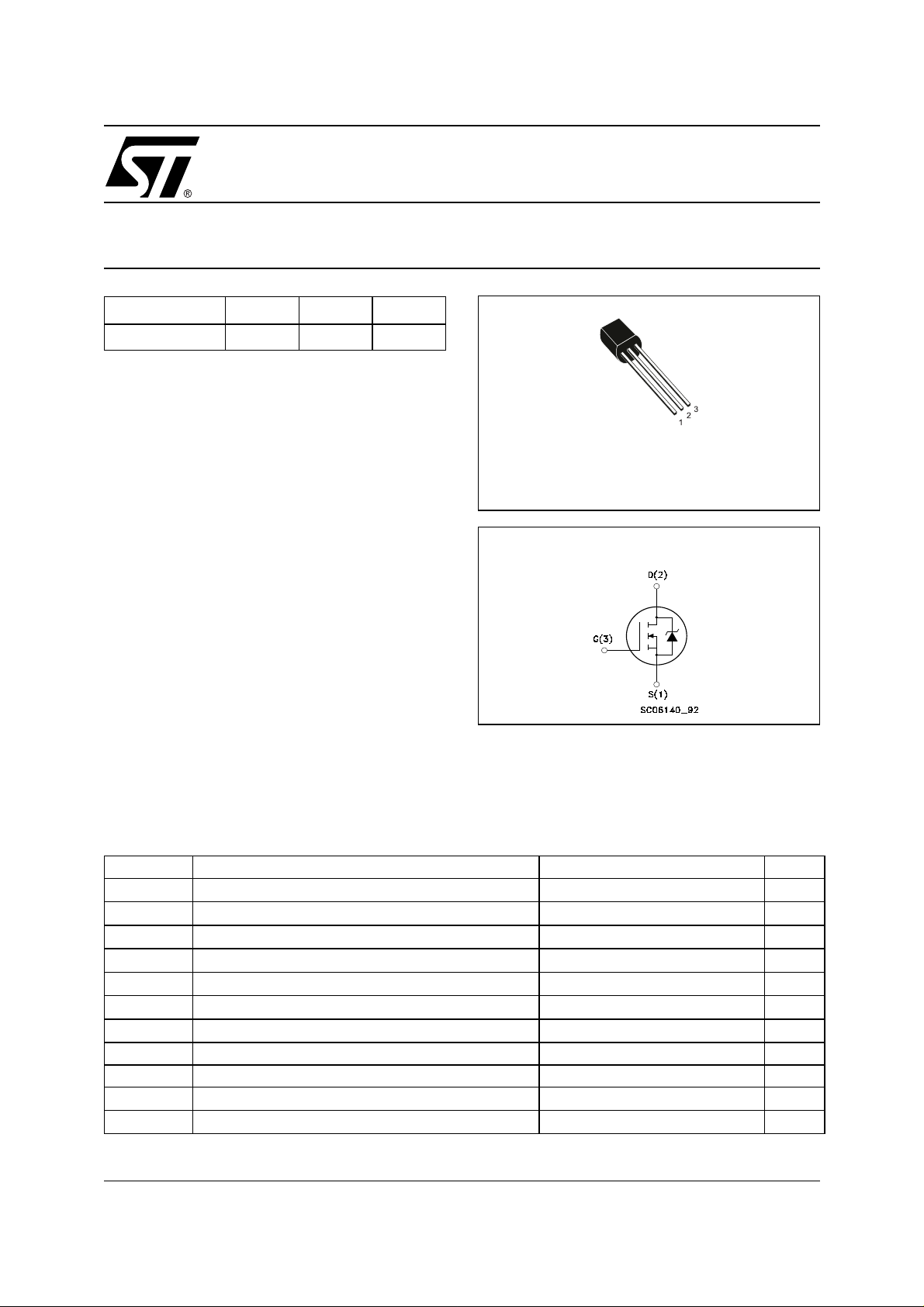
TO-92
INTERNAL SCHEMATIC DIAGRAM
ABSOLUTE MAXIMUM RATINGS
Symbol Parameter Value Unit
V
DS
V
DGR
V
GS
I
D
I
D
I
DM
P
TOT
dv/dt(1) Peak Diode Recovery voltage slope 3.5 V/ns
T
stg
T
(•)Pu l se width limited by safe operating area
August 2001
Drain-source Voltage (VGS = 0)
Drain-gate Voltage (RGS = 20 kΩ)
600 V
600 V
Gate- source Voltage ± 30 V
Drain Current (continuos) at TC = 25°C
Drain Current (continuos) at TC = 100°C
(●)
Drain Current (pulsed) 1.6 A
Total Dissipation at TC = 25°C
0.4 A
0.25 A
3.5 W
Derating Factor 0.028 W/°C
Storage Temperature –65 to 150 °C
Max. Operating Junction Temperature 150 °C
j
(1)ISD ≤ 0.4 A, di/dt ≤100A/µs, VDD ≤ V
(BR)DSS
, Tj ≤ T
JMAX.
1/6
STQ1HNC60
THERMA L D ATA
Rthj-case
Rthj-amb
Thermal Resistance Junction-case
Thermal Resistance Junction-ambient Max
(Surface Mounted)
T
l
Maximum Lead Temperature For Soldering Purpose
AVALANCHE CHARACTERISTICS
Symbol Parameter Max Value Unit
I
AR
E
AS
Avalanche Current, Repetitive or Not-Repetitive
(pulse width limited by T
max)
j
Single Pulse Avalanche Energy
(starting T
= 25 °C, ID = IAR, VDD = 50 V)
j
ELECTRICAL CHARACTERISTICS (TCASE = 25 °C UNLESS OTHERWISE SPECIFIED)
OFF
Symbol Parameter Test Conditions Min. Typ. Max. Unit
V
(BR)DSS
I
DSS
I
GSS
Drain-source
Breakdown Voltage
Zero Gate Voltage
Drain Current (V
GS
Gate-body Leakage
Current (V
DS
= 0)
= 0)
ID = 250 µA, VGS = 0 600 V
V
= Max Rating
DS
V
= Max Rating, TC = 125 °C
DS
V
= ± 30V ±100 nA
GS
35.7
60
300
0.4 A
100 mJ
1µA
50 µA
°C/W
°C/W
°C
ON
(1)
Symbol Parameter Test Conditions Min. Typ. Max. Unit
V
V
GS(th)
R
DS(on)
Gate Threshold Voltage
Static Drain-source On
= VGS, ID = 250 µA
DS
= 10V, ID = 0.4 A
V
GS
234V
78Ω
Resistance
DYNAMIC
Symbol Parameter Test Conditions Min. Typ. Max. Unit
g
fs
Forward Transconductance VDS > I
ID= 0.4 A
C
iss
C
oss
C
rss
Input Capacitance
Output Capacitance 26 pF
Reverse Transfer
V
DS
Capacitance
x R
D(on)
DS(on)max,
= 25V, f = 1 MHz, VGS = 0
1.25 S
160 pF
3.8 pF
2/6
 Loading...