

SGS Thomson Microelectronics STPS2545CG, STPS2545CFP Datasheet
®
STPS2545CT/CG/CFP
POWER SCHOTTKY RECTIFIER
MAIN PRODUCT CHARACTERISTICS
I
F(AV)
V
RRM
2 x 12.5 A
45 V
Tj (max) 175 °C
V
(max) 0.57V
F
FEATURES AND BENEFITS
VERY SMALL CONDUCTION LOSSES
■
NEGLIGIBLE SWITCHING LOSSES
■
EXTREMELY FAST SWITCHING
■
LOW THERMAL RESISTANCE
■
AVALANCHE CAPABILITY SPECIFIED
■
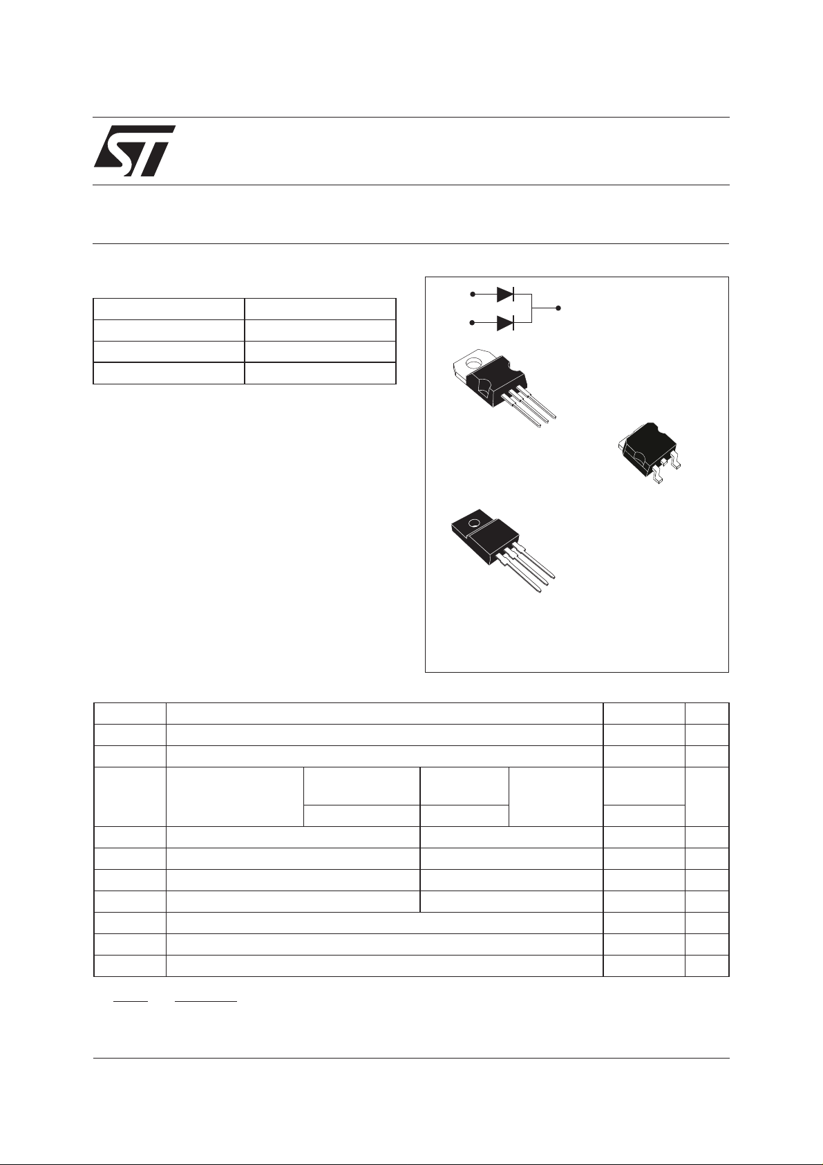
DESCRIPTION
Dual center tap Schottky rectifier suited for
Switch Mode Power Supplies and high frequency DC to DC converters.
This device is especially intended for use in low
voltage, high frequency inverters, free wheeling
and polarity protection applications.
ABSOLUTE RATINGS (limiting values, per diode)
A1
A2
TO-220AB
STPS2545CT
TO-220FPAB
STPS2545CFP
A1
A1
K
A2
K
K
A2
A1
D2PAK
STPS2545CG
A2
K
Symbol Parameter Value Unit
V
RRM
I
F(RMS)
I
F(AV)
Repetitive peak reverse voltage 45 V
RMS forward current 30 A
Average forward
current δ = 0.5
TO-220AB
D2PAK
Tc = 160°C Per diode 12.5 A
TO-220FPAB Tc = 140°C Per device 25
I
I
I
P
T
FSM
RRM
RSM
ARM
stg
Surge non repetitive forward current tp = 10 ms sinusoidal 200 A
Repetitive peak reverse current tp=2µssquare F = 1kHz 1 A
Non repetitive peak reverse current tp = 100 µs square 2 A
Repetitive peak avalanche power tp = 1µs Tj = 25°C 4800 W
Storage temperature range -65 to+175 °C
Tj Maximum operating junction temperature * 175 °C
dV/dt Critical rate of rise of reverse voltage 10000 V/µs
dPtot
* :
<
dTj Rth j a
July 2003 - Ed: 2A
thermal runaway condition for a diode on its own heatsink
−1()
1/6

STPS2545CT/CG/CFP
THERMAL RESISTANCES
Symbol Parameter Value Unit
R
th (j-c)
R
th (c)
When the diodes 1 and 2 are used simultaneously :
∆ Tj(diode 1) = P(diode1) x R
STATIC ELECTRICAL CHARACTERISTICS (per diode)
Symbol Parameter Tests Conditions Min. Typ. Max. Unit
I
R
V
Pulse test : * tp = 380 µs, δ <2%
To evaluate the conduction losses use the following equation :
P = 0.42 x I
Fig.1: Conduction losses versusaverage current.
P (W)F(AV)
10
9
8
7
6
5
4
3
2
1
0
0.0 2.5 5.0 7.5 10.0 12.5 15.0
Junction to ambient TO-220AB / D2PAK Per diode 1.6 °C/W
TO-220FPAB 4
TO-220AB / D
2
PAK Total 1.1 °C/W
TO-220FPAB 3.5
TO-220AB / D2PAK
Coupling
0.6 °C/W
TO-220FPAB 3
(Per diode) + P(diode 2) x R
th(j-c)
* Reverse leakage Current Tj = 25°C VR=V
th(c)
RRM
125 µA
Tj = 125°C 9 25 mA
* Forward Voltage drop Tj = 125°C IF= 12.5 A 0.50 0.57 V
F
F(AV)
+ 0.012 x I
Tj = 25°C I
Tj = 125°C I
F2(RMS)
= 25 A 0.84
F
= 25 A 0.65 0.72
F
Fig. 2: Average forward current versus ambient
temperature (δ=0.5).
I (A)F(AV)
δ = 0.05
δ = 0.1
I (A)F(AV)
δ = 0.2
δ = 0.5
δ
=tp/T
T
δ = 1
14
12
10
8
6
4
2
tp
δ
0
0 25 50 75 100 125 150 175
=tp/T
Rth
=Rth
(j-a)
(j-c)
Rth
=50°C/W
(j-a)
T
tp
T (°C)amb
TO-220AB/D²PAK
Fig. 3: Normalized avalanche power derating
versus pulse duration.
P(t)
ARM p
P (1µs)
ARM
1
0.1
0.01
t (µs)
0.001
0.10.01 1
2/6
p
10 100 1000
Fig. 4: Normalized avalanche power derating
versus junction temperature.
P(t)
ARM p
P (25°C)
ARM
1.2
1
0.8
0.6
0.4
0.2
0
0 25 50 75 100 125 150
T (°C)
j
 Loading...