

SGS Thomson Microelectronics STPIC6C595TTR, STPIC6C595MTR, STPIC6C595M Datasheet
STPIC6C595
POWER LOGIC 8-BIT SHIFT REGISTER
■ LOW R
■ 30mJ AVAILANCHE ENERGY
■ EIGHT 100mA DMOS OUTPUTS
■ 250mA CURRENT LIMIT CAPABILITY
■ 33V OUTPUT CLAMP VOLTAGE
■ DEVICE ARE CASCADABLE
■ LOW POWER CONSUMPTION
DS(on)
:4ΩTYP
DESCRIPTION
This STPIC6C595 is a monolithic,
medium-voltage, low current power 8-bit s hift
register designed for use in systems that require
relatively moderate l oad power such as LEDs. The
device contains a built-in voltage clamp on the
outputs for inductive transient protection. Power
driver application s include relays, solenoids, and
other low-current or medium-voltage loads.
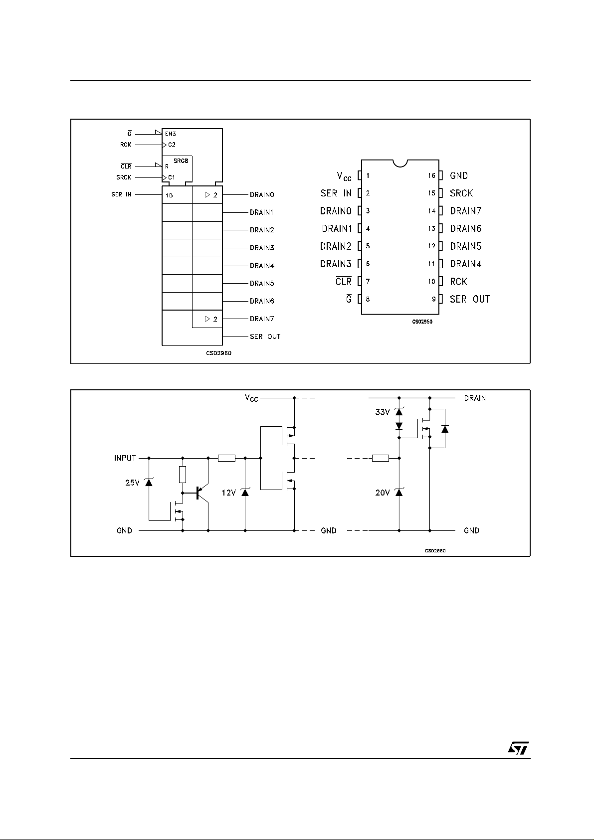
The device c ontains an 8-bit serial-in, parallel-out
shift regist er that feeds an 8-bit D-type s tora ge
register. Data transfe rs through both the shift and
storage register clock (SRCK) and the register
clock (RCK
), respectively. The device transfers
data out the serial output (SER OUT) port on the
rising edge of SRCK. The storage register
transfers data to the output buffer when shift
register c lear (CLR) is high. When CLR
is low, the
input shift register is cleared. When output enable
(G
) is held high, all data in the output buf fer is held
low and all drain output are of f. When G is held
low, data from the storage register is t r ans parent
to the output buffer. When data in the output
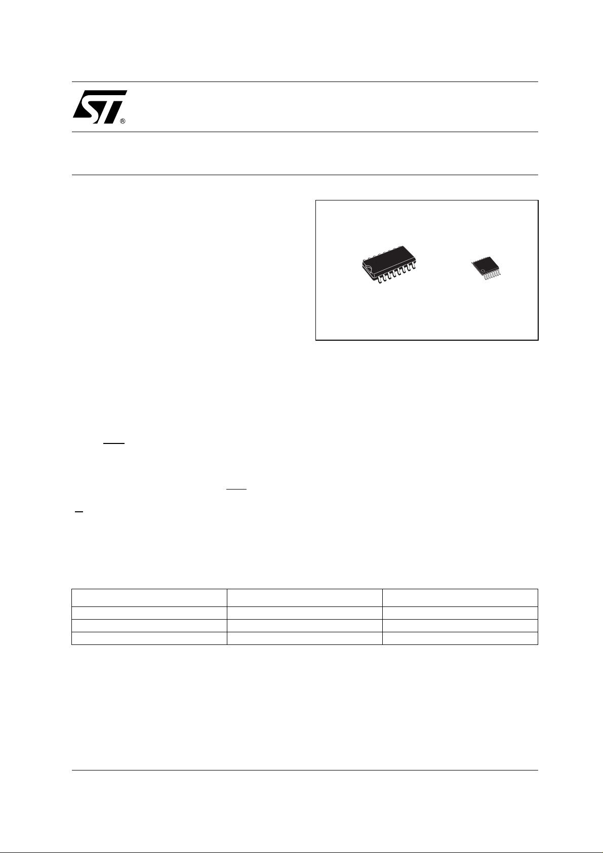
SOP TSSOP
buffers is low, the DMOS transi stor outputs are off.
When data is high, the D MOS transistor outputs
have sink-c urrent capability. The SER OUT allows
for cascading of the data from the shift register to
additional devices.
Output are low-side, open-drain DMOS transistors
with output ratings of 33V and 100mA continuous
sink-current capability. Each output provides a
250 mA maximum current limit at T
= 25°C. The
C
current limit decreases as the junction
temperature increases for additional d ev ice
protection. The device also provides up to 1.5KV
of ESD protection when tested using the
human-body model and 200V machine model.
The STPIC6C595 is c harac terized for operation
over the operating case temperature range of
-40°C to 125°C.
ORDERING CODES
Type Package Comments
STPIC6C595M SO-16 (Tube) 50parts per tube / 20tube per box
STPIC6C595MTR SO-16 (Tape & Reel) 2500 parts per reel
STPIC6C595TTR TSSOP16 (Tape & Reel) 2500 parts per reel
1/14August 2002
STPIC6C595
Figure1 : Logic Symbol And Pin Configuration
Figure2 : Input And Output Equivalent Circuits
2/14
STPIC6C595
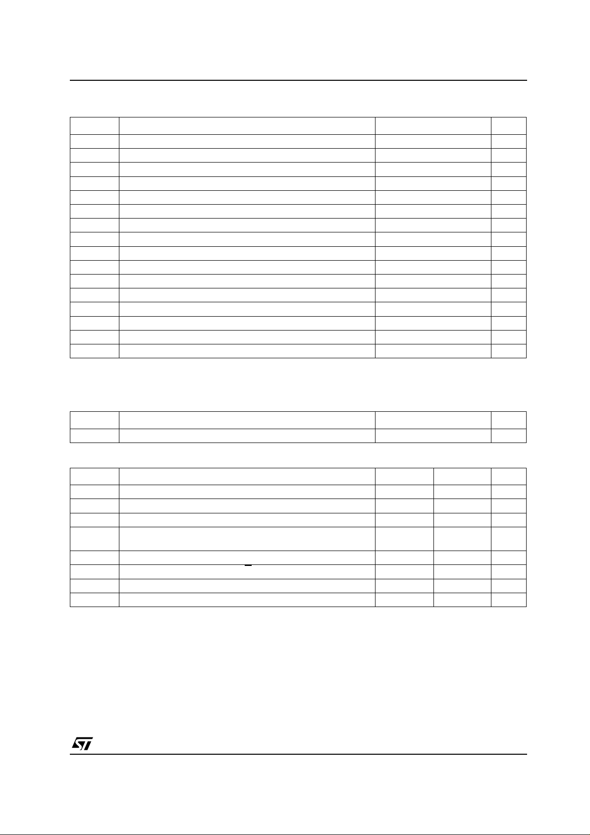
ABSOLUTE MAXIMUM RATINGS
Symbol Parameter Value Unit
V
V
V
I
DS
I
DS
I
I
I
E
I
AS
P
P
T
T
T
T
Absolute Maximum Ratings are those values beyond which damage to the device may occur. Functional operation under these condition is
not implied.
Logic Supply Voltage (See Note 1)
CC
Logic Input Voltage Range
I
Power DMOS Drain to Source Voltage (See Note 2)
DS
Continuous Source to Drain Diode Anode Current
Pulsed Source to Drain Diode Anode Current (See Note 3)
Pulsed Drain Current, Each Output, All Output ON (TC=25°C)
D
Continuous Current, Each Output, All Output ON (TC=25°C)
D
Peak Drain Current Single Output (TC=25°C) (See Note 3)
D
Single Pulse Avalanche Energy (See Figure11 and 12)
AS
Avalanche Current (See Note 4 and figure 17)
Continuous total dissipation (TC≤ 25°C)
d
Continuous total dissipation (TC= 125°C)
d
Operating Virtual Junction Temperature Range
J
Operating Case Temperature Range
C
Storage Temperature Range
stg
Lead Temperature 1.6mm (1/16inch) from case for 10 seconds
L
7V
-0.3 to 7 V
33 V
250 mA
500 mA
250 mA
100 mA
250 mA
30 mJ
200 mA
1087 mW
217 mW
-40 to +150 °C
-40 to +125 °C
-65 to +150 °C
260 °C
THERMAL DATA
Symbol Parameter Value Unit
R
thj-amb
Thermal Resistance Junction-ambient
115 °C/W
RECOMMENDED OPERATING CONDITIONS
Symbol Parameter Min. Max. Unit
V
V
V
I
DP
t
t
t
T
Logic Supply Voltage 4.5 5.5 V
CC
High Level Input Voltage 0.85V
IH
Low Level Input Voltage 0 0.15V
IL
CC
Pulse Drain Output Current (TC=25°C, VCC=5V,all outputs ON)
(see note 3, 5 and figure 15)
Set-up Time, SER IN High Before SRCK ↑ (see Figure 6 and 8) 20 ns
su
Hold Time, SER IN High Before G ↑ (see Figure 6, 7, 8) 20 ns
h
Pulse Duration (see Figure 8) 40 ns
W
Operating Case Temperature -40 125 °C
C
V
CC
CC
250 mA
V
V
3/14
STPIC6C595
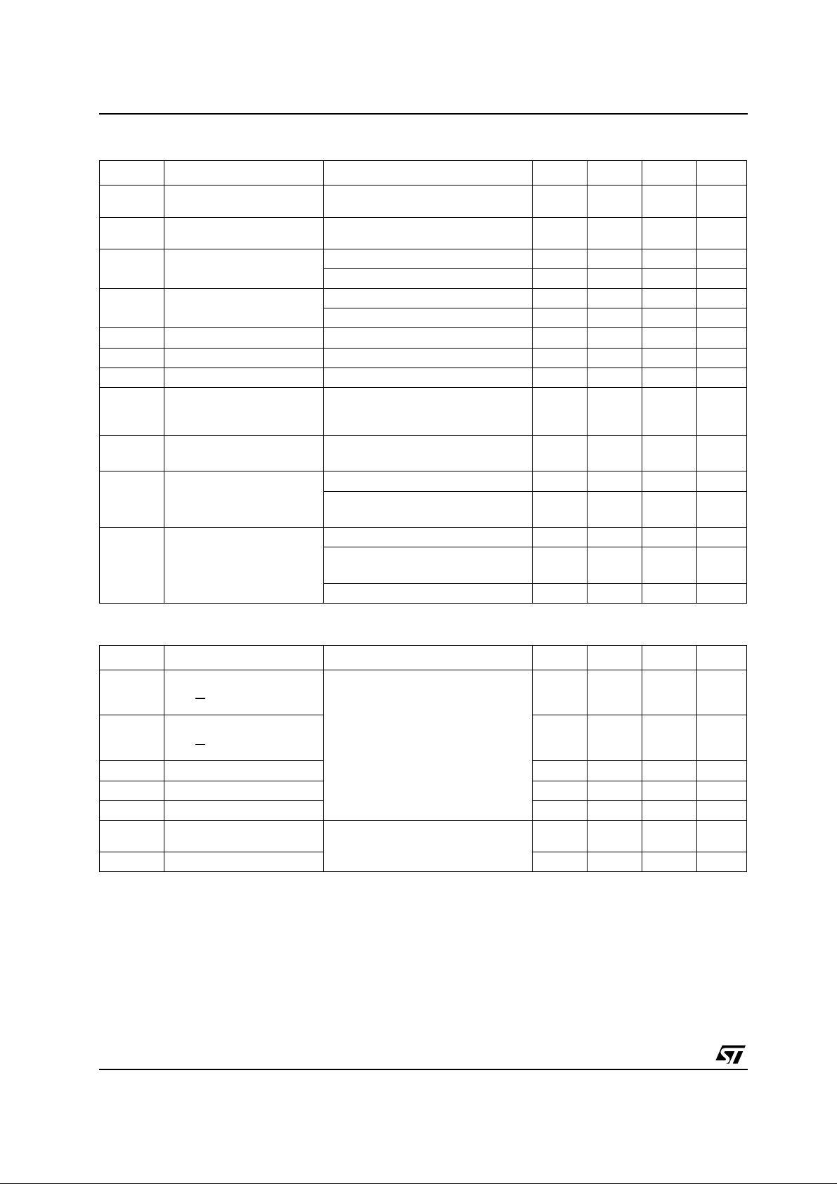
DC CHARACTERISTICS (VCC=5V, TC= 25°C, unless otherwise specified.)
Symbol Parameter Test Conditions Min. Typ. Max. Unit
V
(BR)DSX
V
SD
V
OH
V
OL
I
IH
I
IL
I
CC
I
CC(FRQ)
I
N
I
DSX
R
DS(on)
Drain-to-Source breakdown
Voltage
Source-to-Drain Diode
Forward Voltage
High Level Output Voltage
SER OUT
Low Level Output Voltage
SER OUT
High Level Input Current VCC= 5.5V VI=V
Low Level Input Current VCC= 5.5V VI=0 -1 µA
Logic Supply Current VCC= 5.5V All outputs OFF or ON 20 200 µA
Logic Supply Current at
Frequency
Nominal Current V
Off-State Drain Current VDS= 30V VCC= 5.5V 0.3 5 µA
Static Drain Source ON
StateResistance (See Note
5, 6 and figg. 14, 16)
ID= 1mA 33 37 V
IF= 100 mA 0.85 1.2 V
IOH=-20µAVCC= 4.5V 4.4 4.49 V
=-4mA VCC= 4.5V 4 4.2 V
I
OH
IOH=20µAVCC= 4.5V 0.005 0.1 V
= 4 mA VCC= 4.5V 0.3 0.5 V
I
OH
1 µA
f
= 5MHz CL= 30pF
SRCK
CC
0.2 2 mA
All outputs OFF
(See Figg. 6, 18 and 19)
= 0.5V IN=I
DS(on)
D
90 mA
TC=85°C (See Note 5, 6, 7)
= 30V VCC=5.5V or 0V
V
DS
T
=125°C
C
0.6 8 µA
ID= 50mA VCC= 4.5V 4.5 6 Ω
= 50mA VCC= 4.5V
I
D
T
=125°C
C
= 100mA VCC= 4.5V 4.5 6 Ω
I
D
6.5 9 Ω
SWITCHING CHARACTERISTICS (V
=5V, TC= 25°C, unless otherwise specified.)
CC
Symbol Parameter Test Conditions Min. Typ. Max. Unit
t
PHL
Propagation Dealy Time,
High to Low Level Output
CL=30pF ID= 75mA
(See Figg. 4, 5, 6,7, 20)
80 ns
from G
t
PLH
Propagation Dealy Time,
Low to High Level Output
130 ns
from G
Rise Time, Drain Output 60 ns
t
r
Fall Time, Drain Output 50 ns
t
f
t
Note 1: All Voltage value are with respect to GND
Note 2: Each power DMOS source is internally connected to GND
Note 3: Pulse duration ≤ 100µs and duty cycle ≤ 2%
Note 4: Drain Supply Voltage = 15V, starting junction temperature (T
Note 5: Technique should limit T
Note 6: These parameters are measured with voltage sensing contacts separate from the current-carrying contacts.
Note 7: Nominal Current is defined for a consistent comparison between devices from different sources. It is the current that produces a
voltagedropof0.5VatT
propagation Delay Time 20 ns
pd
Reverse Recovery Current
t
a
Rise Time
Reverse Recovery Time 115 ns
t
rr
to 10°C maximum
J-TC
=85°C.
C
IF= 100mA di/dt = 10A/µs
(See Note 5, 6 and Fig. 9 and 10)
) = 25°C. L = 1.5H and IAS= 200mA (See Fig. 11 and 12)
JS
39 ns
4/14

Figure3 : Logic Diagram
STPIC6C595
5/14
 Loading...