

SGS Thomson Microelectronics STPIC6A259MTR, STPIC6A259M Datasheet
POWER LOGIC 8-BIT ADDRESSABLE LATCH
■ LOW R
■ OUTPUT SHORT-CI RCUIT PROTECTION
■ 75mJ AVAILANCHE ENERGY
■ EIGHT 350mA DMOS OUTPUTS
■ 50V SWITCHING CAPABILITY
■ FOUR DISTINCT FUNCTION MODES
■ LOW POWER CONSUMPTION
DS(on)
: 1Ω TYP
STPIC6A259
PRELIMINARY DATA
DESCRIPTION
This power logic 8-bit addressable latch cont rols
open-drain DMOS transistor outputs and is
designed for general-purpose storage
applications in digital systems. Specific uses
include working registers, serial-holding registers,
and decoders or demultiplexers. This is a
multifunctional device capable of operating as
eight addressable latches or an 8-line
demultiplexer with active-low DMOS outputs.
Each open-drain DMOS transistor features an
independent chopping current-limiting circuit to
prevent damage in the case of a short circuit.
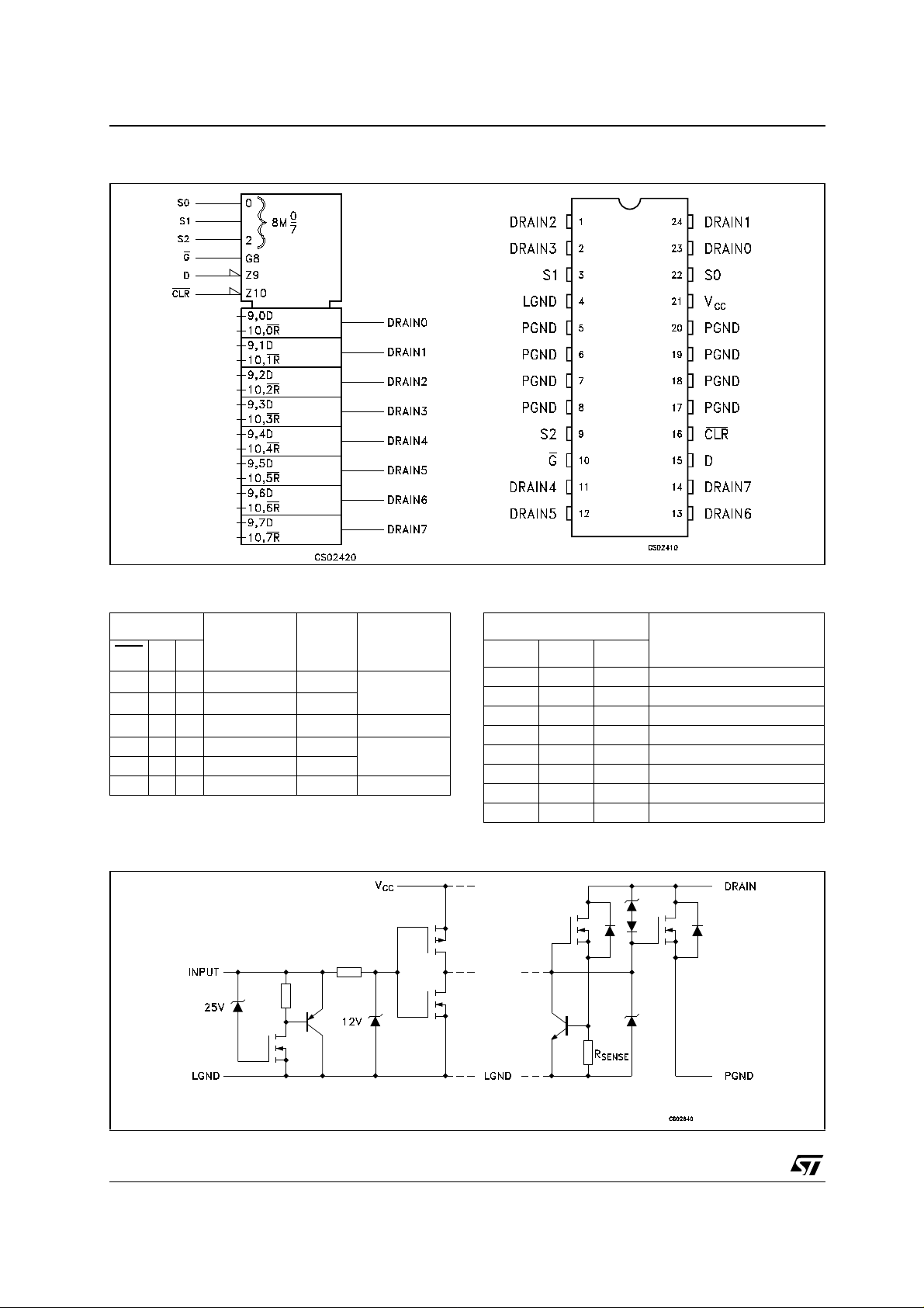
Four distinct modes of operation are selectable by
controlling the clear (CLR
) and enable ( G) inputs
and enumerated in the function table. In the
addressable-latch mode, data at the data-in (D)
terminal is written into the addressed latch. The
addressed DMOS-transistor output inverts the
data input with all unadressed DMOS-transistor
output remaining in their previuous state. In the
MOS-transistor outputs remain in their previous
states and are unaffecte d by the data or address
inputs. To eliminate the possibility of entering
erroneus data in the latch, enable G should be
SOP
held high (inactive) while the address lines are
changing. In the 8-line demoul tiplexing mode, the
addressed output is inverted with res pectto the D
input and all other output are high. In the clear
mode, all out puts are high an d unaffected b y the
address and data inputs.
Separate power ground (PGND) and logic ground
(LGND) terminals are providied to facilitate
maximum system flexibility. All PGND terminals
are interally connected, and eac h pGND terminal
must be externally connected to the power system
ground in o rder to minimize parasit ic impedance.
A single-point connection between LGND and
PGND must b e mad e external ly in a m anner t hat
reduces crosstalk between the logi and load
circuits.
The STPIC6A259 is offered in a termally
enhanced SO-24 package. The STPIC6A259 is
characterized for operation over the operating
case temperature range -40°C to 125°C.
ORDERING CODES
Type Package Comments
STPIC6A259M SO-24 Batwing (Tube) 50parts per tube / 20tube per box
STPIC6A259MTR SO-24 Batwing (Tape & Reel) 2500 parts per reel
1/13March 2001
This is preliminary information on a new product now in development are or undergoing evaluation. Details subject to change without notice.
STPIC6A259
LOGIC SYMBOL AND PIN CONFIGURATION
FUNCTIONAL TABL E FUNCTIONAL TABLE
INPUTS OUTPUT OF
GD
CLR
HLH L Q
HLL H Q
HHX Q
L L H L H 8-Line
LLL H H
L H X H H Clear
ADDRESSED
DRAIN
io
EACH
OTHER
DRAIN
io
io
Q
io
FUNCTION
Addressable
Latch
Memory
Demultiplexer
SELECT INPUTS
S2 S1 S0
LLL 0
LLH 1
LHL 2
LHH 3
HLL 4
HLH 5
HHL 6
HHH 7
INPUT AND OUTPUT EQUIVALENT CIRCUITS
DRAIN ADDRESSED
2/13
STPIC6A259
ABSOLUTE MAXIMUM RATINGS
Symbol Parameter Value Unit
V
V
V
I
DS
I
DS
I
I
I
E
I
AS
P
P
T
T
T
T
Logic Supply Voltage (See Note 2)
CC
Logic Input Voltage Range
I
Power DMOS Drain to Source Voltage (See Note 2)
DS
Continuous Source to Drain Diode Anode Current
Pulsed Source to Drain Diode Anode Current (See Note 3)
Pulsed Drain Current, Each Output, All Output ON (TC=25°C)
D
Continuous Current, Each Output, All Output ON (TC=25°C)
D
Peak Drain Current Single Output (TC=25°C) (See Note 3)
D
Single Pulse Avalanche Energy (See Note 6)
AS
Avalanche Current (See Note 4)
Continuous total dissipation (TC ≤ 25°C)
d
Continuous total dissipation (TC = 125°C)
d
Operating Virtual Junction Temperature Range
J
Operating Case Temperature Range
C
Storage Temperature Range
stg
Lead Temperature 1.6mm (1/16inch) from case for 10 seconds
L
7V
-0.3 to 7 V
50 V
1A
2A
1.1 A
350 mA
1.1 A
75 mJ
600 mA
1750 mW
350 mW
-40 to +150 °C
-40 to +125 °C
-65 to +150 °C
260 °C
Absolute Maximum Ratings are those values beyond which damage to the device may occur. Functional operation under these condition i s
not implied.
THERMAL DATA
Symbol Parameter Unit
R
thj-case
R
thj-amb
Thermal Resistance Junction-case
Thermal Resistance Junction-ambient
10 °C/W
50 °C/W
RECOMMENDED OPERATING CONDITIONS
Symbol Parameter Min. Max. Unit
V
V
V
I
DP
t
t
t
T
Logic Supply Voltage 4.5 5.5 V
CC
High Level Input Voltage 0.85V
IH
Low Level Input Voltage 0 0.15V
IL
CC
Pulse Drain Output Current (TC=25°C, VCC=5V) (see note 3, 5) -1.8 0.6 A
Set-up Time, D High Before G ↑ (see Figure 2) 10 ns
su
Hold Time, D High Before G ↑ (see Figure 2) 5 ns
h
Pulse Duration (see Figure 2) 15 ns
W
Operating Case Temperature -40 125 °C
C
V
CC
CC
V
V
3/13
STPIC6A259
DC CHARACTERISTICS (VCC=5V, TC= 25°C, unless otherwise specified.)
Symbol Parameter Test Conditions Min. Typ. Max. Unit
V
(BR)DSX
V
I
I
I
I
(nom)
R
DS(on)
Drain-to-Source breakdown
ID = 1mA 50 V
Voltage
Source-to-Drain Diode
SD
Forward Voltage
High Level Input Current VI = V
IH
I
Low Level Input Current VI = 0 -1 µA
IL
Logic Supply Current IO = 0 0.5 5 mA
CC
Output Current at Which
OK
Chopping Starts
Nominal Current V
IF = 350 mA (See Note 3) 0.8 1.1 V
CC
TC = 25°C (See Note 3 and Figg.
0.6 0.8 1.1 A
3, 4)
= 0.5V I
DS(on)
(nom)
= I
D
350 mA
VCC = 5V TC=85°C
(See Note 5, 6, 7)
I
Off-State Drain Current VDS = 40V TC=25°C 0.1 1 µA
D
V
= 40V TC=125°C 0.2 5 µA
DS
Termination Resistance
(See Note 5, 6 and figg. 9,
10)
ID = 350mA TC=25°C 1 1.5 Ω
I
= 350mA TC=125°C 1.7 2.5 Ω
D
1 µA
SWITCHING CHARACTERISTICS (V
=5V, TC= 25°C, unless otherwise specified.)
CC
Symbol Parameter Test Conditions Min. Typ. Max. Unit
t
PHL
Propagation Dealy Time,
High to Low Level Output
CL = 30pF ID = 350mA
(See Figg. 1, 2, 11)
30 ns
from D
t
PLH
Propagation Dealy Time,
Low to High Level Output
125 ns
from D
t
Rise Time, Drain Output 60 ns
r
t
Fall Time, Drain Output 30 ns
f
t
Reverse Recovery Current
a
Rise Time
t
Reverse Recovery Time 300 ns
rr
Note 1: A l l Vol tage valuea are with res pect to LGN D and PGND
Note 2: Each power DMOS source is inte rnally connected to GND
Note 3: Pul se duration ≤ 100ms
Note 4: Dr ai n Supply Voltage = 15V, start i ng junction t em perature (T
Note 5: Technique should limit T
Note 6: These paramet ers are measured with voltage sensing contacts separate from the current-carrying contacts.
Note 7: No minal Current i s defined for a consistent co m parison betw een devices f rom different sources. It is th e current that p roduces a
voltage drop of 0.5V at T
and duty cy cl e ≤ 2%
- TC to 10°C maximum
J
= 85°C.
C
IF = 350mA di/dt = 20A/µs
(See Note 5, 6 and Fig. 5)
) = 25°C. L = 210µ H and IAS = 600mA (See Fig. 6)
JS
100 ns
4/13
 Loading...