

SGS Thomson Microelectronics STPCD01 Datasheet
Issue 1.7 1/48
STPC CLIENT
PC Compatible Embedded Microprocessor
February 8, 2000
Figure 1. Logic Diagram
• POWERFUL X86 PROCESSOR
• 64-BIT 66MHz BUS INTERFACE
• 64-BIT DRAM CONTROLLER
• SVGAGRAPHICS CONTROLLER
• UMA ARCHITECTURE
• VIDEO SCALER
• VIDEO OUTPUT PORT
• VIDEO INPUT PORT
• CRT CONTROLLER
• 135MHz RAMDAC
• 2 OR 3 LINEFLICKER FILTER
• SCAN CONVERTER
• PCI MASTER / SLAVE / ARBITER
• ISA MASTER/SLAVE
• IDE CONTROLLER
• DMA CONTROLLER
• INTERRUPT CONTROLLER
• TIMER / COUNTERS
• POWER MANAGEMENT
STPC CLIENT OVERVIEW
The STPC Client integrates a standard 5th
generation x86 core, a DRAM controller, a
graphics subsystem, a video pipeline, and
support logic including PCI, ISA, and IDE
controllers to provide a single Consumer
orientated PC compatible subsystem on a single
device.
The device is based on a tightly coupled Unified
Memory Architecture (UMA), sharing the same
memory array between the CPU main memory
and the graphics and video frame buffers.
Extra facilities are implemented to handle video
streams. Features include smooth scaling and
colour space conversion of the video input stream
and mixing of the video stream with non-video
data from the frame buffer. The chip also includes
anti-flicker filters to provide a stable, high-quality
Digital TV output.
The STPC Client is packaged in a 388 Plastic Ball
Grid Array (PBGA).
PBGA388
x86
Core
Host I/F
DRAM
VIP
PCI
PCIBUS
ISA
EID
PCI
ISABUS
CRT
HW
Monitor
TVOutput
SYNCOutput
Col-
Col-
our
Vid-
CCIRInput
EIDE
2D
Anti-
IPC

STPC CLIENT
2/48 Issue 1.7 - February 8, 2000
• X86 Processor core
• Fully static 32-bit 5-stage pipeline, x86 proc-
essor with DOS, Windows and UNIX compatibility.
• Can access up to 4GB of external memory.
• KBytes unified instruction and data cache
with write back and write through capability.
• Parallelprocessingintegralfloating point unit,
with automatic power down.
• Clock core speeds up to of 75 MHz.
• Fully static design for dynamic clock control.
• Low power and system management modes.
• Optimized design for 3.3V operation.
• DRAM Controller
• Integrated system memory andgraphic frame
memory.
• Supports up to 128 MBytes system memory
in 4 banks and as little as MBytes.
• Supports 4MBytes, 8MBites, 16MBites,
32MBites single-sided and double-sided
DRAM SIMMs.
• Four quad-word write buffers for CPU to
DRAM and PCI to DRAM cycles.
• Four 4-word read buffers for PCI masters.
• Supports Fast Page Mode & EDO DRAMs.
• Programmable timing for DRAM parameters
including CAS pulse width, CAS pre-charge
time, and RAS to CAS delay.
• 60, 70, 80 & 100ns DRAM speeds.
• Memory hole size of 1 MByte to 8 MBytes
supported for PCI/ISA buses.
• Hidden refresh.
To check if your memory device is supported by
the STPC, please refer to Table 7-69 in the
Programming Manual.
• Graphics Controller
• 64-bit windows accelerator.
• Backward compatibility to SVGA standards.
• Hardware acceleration for text, bitblts, trans-
parent blts and fills.
• Up to 64 x 64 bit graphics hardware cursor.
• Up to 4MB long linear frame buffer.
• 8-, 16-, and 24-bit pixels.
• CRT Controller
• Integrated 135MHz triple RAMDACallowing
up to 1024 x 768 x 75Hz display.
• 8-, 16-, 24-bit per pixels.
• Interlaced or non-interlaced output.
• Video Pipeline
• Two-tapinterpolative horizontal filter.
• Two-tapinterpolative vertical filter.
• Colour space conversion (RGB to YUV and
YUV to RGB).
• Programmable window size.
• Chroma and colour keying allowing video
overlay.
• Programmable two tap filter with gamma correction or three tap flicker filter.
• Progressiveto interlaced scan converter.
• Video Input port
• Decodes video inputs in ITU-R 601/656 com-
patible formats.
• Optional 2:1 decimator
• Stores captured video in off setting area of
the onboard frame buffer.
• Video pass through to the onboard PAL/
NTSC encoder for full screen video images.
• HSYNC and B/T generation or lock onto
external video timing source.
• PCI Controller
• Integrated PCI arbitrationinterface able to
directly manage up to 3 PCI masters at a
time.
• Translation of PCI cycles to ISA bus.
• Translation of ISA master initiated cycle to
PCI.
• Support for burst read/write from PCI master.
• The PCI clock runs at a third or half CPU
clock speed.

STPC CLIENT
Issue 1.7 - February 8, 2000 3/48
• ISA master/slave
• The ISA clock generated from either
14.318MHz oscillator clock or PCI clock
• Supports programmable extra wait state for
ISA cycles
• Supports I/O recovery time for back to back I/
O cycles.
• Fast Gate A20 and Fast reset.
• Supports the single ROM that C, D,or E.
blocks shares with F block BIOS ROM.
• Supports flash ROM.
• Buffered DMA & ISA master cycles to reduce
bandwidth utilizationofthe PCI and Host bus.
• IDE Interface
• Supports PIO
• Supports up to Mode 5 Timings
• Supports up to 4 IDE devices
• Individual drive timing for all four IDEdevices
• Concurrent channel operation (PIO modes) -
4 x 32-Bit Buffer FIFO per channel
• Support for PIO mode 3 & 4
• Support for 11.1/16.6 MB/s, I/O Channel
Ready PIO data transfers.
• Supports both legacy & native IDE modes
• Supports hard drives larger than 528MB
• Support for CD-ROM and tape peripherals
• Backward compatibility with IDE (ATA-1).
• Integrated peripheral controller
• 2X8237/AT compatible 7-channel DMA con-
troller.
• 2X8259/AT compatible interrupt Controller.
16 interrupt inputs - ISA and PCI.
• Three 8254 compatible Timer/Counters.
• Power Management
• Four power saving modes: On, Doze, Stand-
by, Suspend.
• Programmable system activity detector
• Supports SMM.
• Supports STOPCLK.
• Supports IO trap & restart.
• Independent peripheral time-out timer to
monitor hard disk, serial & parallel ports.
• Supports RTC, interrupts and DMAs wake-up

STPC CLIENT
4/48 Issue 1.7 - February 8, 2000

UPDATE HISTORY FOR OVERVIEW
Issue 1.7 - February 8, 2000 5/48
UPDATE HISTORY FOR OVERVIEW
The following changes have been made to the Board LayoutChapter on 02/02/2000.
The following changes have been made to the Board LayoutChapter from Revision 1.0 to Release 1.2.
Section Change Text
Added
To check if your memory device is supported by the STPC, please refer to
Table 7-69 Host Address to MA Bus Mappingin the Programming Manual.
Section Change Text
N/A Replaced
“fully PC compatible” With “with DOS, Windows and UNIX compatibility”
N/A Replaced “133 MHz” With 75 MHz”
N/A Removed
“Drivers for Windows and other operating systems.”
N/A Removed
“
Requires external frequency synthesizer and reference sources.”
N/A Replaced
“
Chroma and colour keying for integrated video overlay.” With “Chroma and colour
keying
allowing video overlay.
N/A Replaced
“Accepts video inputs in CCIR 601/656 or ITU-R 601/656, and decodes the
stream.” With “Decodes video inputs in ITU-R 601/656 compatible formats.
N/A Replaced
“Fully compliant with PCI 2.1 specification.
Integrated PCI arbitration interface. Up to 3 masters can connect directly.
External PAL allows for greater than 3 masters.”
With
“Integrated PCI arbitration interface able to directly manage up to 3 PCI
masters at a time.”
N/A Replaced
“0.33X and 0.5X CPU clock PCI clock.” With “The PCI clock runs at a third or
half CPU clock speed.”
N/A Removed
“Supports flash ROM.”
N/A Replaced
“Supports ISA hidden refresh.” With “Supports flash ROM.”
N/A Replaced
“
Buffered DMA & ISA master cycles to reduce bandwidth utilization of the PCI
and Host bus. NSP compliant.” With “Buffered DMA & ISA master cycles to
reduce bandwidth utilization of the PCI and Host bus. “
N/A Replaced
“
Supports PIO and Bus Master IDE” With “Supports PIO”
N/A Removed
“Transfer Rates to 22 MBytes/sec”
N/A Added “Individual drive timing for all four IDE devices “
N/A Replaced
“Concurrent channel operation (PIO & DMA modes) - 4 x 32-Bit Buffer FIFO
per channel”
With
“Concurrent channel operation (PIO modes) - 4 x 32-Bit Buffer FIFO per
channel”
N/A Removed
“Support for DMA mode 1 & 2.”
“Support for 11.1/16.6 MB/s, I/O Channel Ready PIO data transfers.”
“Supports 13.3/16.6 MB/s DMA data transfers”
“Bus Master with scatter/gather capability “
“Multi-word DMA support for fast IDE drives “
“Individual drive timing for all four IDE devices “
“Supports both legacy & native IDE modes”
“Supports hard drives larger than 528MB”
“Support for CD-ROM and tape peripherals”
“Backward compatibility with IDE (ATA-1).”
“Drivers for Windows and other OSes”

UPDATE HISTORY FOR OVERVIEW
6/48 Issue 1.7 - February 8, 2000
N/A Added
“Support for 11.1/16.6 MB/s, I/O Channel Ready PIO data transfers.”
“Supports both legacy & native IDE modes”
“Supports hard drives larger than 528MB”
“Support for CD-ROM and tape peripherals”
“Backward compatibility with IDE (ATA-1).”
N/A Removed
“Co-processor error support logic.”
N/A Replaced “Supports SMM and APM” With “Supports SMM”
N/A Removed
“Slow system clock down to 8MHz”
“Slow Host clock down to 8Hz”
“Slow graphic clock down to 8Hz”
Section Change Text

GENERAL DESCRIPTION
Issue 1.7 - February 8, 2000 7/48
1.GENERAL DESCRIPTION
At the heart of the STPC Client is an advanced
processor block, dubbed the ST X86. The ST X86
includes a powerful x86 processor core along with
a 64-bit DRAM controller, advanced 64bit accelerated graphics and video controller, a high speed
PCI local-bus controller and Industry standard PC
chip set functions (Interrupt controller, DMA Controller, Interval timer and ISA bus) and EIDE controller.
The STPC Client has in addition to the 5ST86 a
Video subsystem and high quality digital Television output.
The STMicroelectronics x86 processorcore is embedded with standard and application specific peripheral modules on the same silicon die. The core
has all the functionality of the ST Microelectronics
standard x86 processor products, including the
low power System Management Mode (SMM).
System Management Mode (SMM) provides an
additional interrupt and address space that can be
used for system power management or software
transparent emulation of peripherals. While running in isolated SMM address space, the SMM interrupt routine can execute without interfering with
the operating system or application programs.
Further power management facilities include a
suspend mode that can be initiated from either
hardware orsoftware.Because of the static nature
of the core, no internal data is lost.
The STPC Client makes use of a tightly coupled
Unified Memory Architecture (UMA), where the
same memory array is used for CPU main memory and graphics frame-buffer. This significantly reduces total system memory with system performances equal to that of a comparable solution with
separate frame buffer and system memory. In addition, memory bandwidth is improved by attaching the graphics engine directly to the 64-bit processor host interface running at the speed of the
processor bus rather than the traditional PCI bus.
The 64-bit wide memory array provides the system with 320MB/s peak bandwidth, double that of
an equivalent system using 32 bits. This allows for
higher screen resolutions and greater colour
depth. The processor bus runs at the speed of the
processor (DX devices) orhalf the speed (DX2 devices).
The ‘standard’ PC chipset functions (DMA, interrupt controller, timers, power management logic)
are integrated with the x86 processor core.
The PCI bus is the main data communication link
to the STPC Client chip. The STPC Client trans-
lates appropriate host bus I/O and Memory cycles
onto the PCI bus. It also supports the generation
of Configuration cycles on the PCI bus. The STPC
Client, as a PCIbus agent (host bridge class), fully
complies with PCI specification 2.1. The chip-set
also implements the PCI mandatory header registers in Type 0 PCI configuration space for easy
porting of PCI aware system BIOS. The device
contains a PCI arbitration function for three external PCI devices.
The STPC Client integrates an ISA bus controller.
Peripheral modules such as parallel and serial
communications ports, keyboard controllers and
additional ISA devices can be accessed by the
STPC Client chip set through this bus.
An industry standard EIDE (ATA 2) controller is
built into the STPC Client and connected internally
via the PCI bus.
Graphics functions are controlled by the on-chip
SVGA controller and the monitor display is managed by the 2D graphics display engine.
This Graphics Engine is tuned to work with the
host CPU to provide a balanced graphics system
with a low silicon area cost. It performs limited
graphics drawing operations, which include hardware acceleration of text, bitblts, transparent blts
and fills. These operations can operate on offscreen or on-screen areas. The frame buffer size
is up to 4 MBytes anywhere in the physical main
memory.
The graphics resolution supported is a maximum
of 1280x1024 in 65536 colours at 75Hz refresh
rate and is VGA and SVGA compatible. Horizontal
timing fields are VGA compatible while the vertical
fields are extended by one bit to accommodate
above display resolution.
STPC Client provides several additional functions
to handle MPEG or similar video streams. The
Video Input Port accepts an encoded digital video
stream in one of a number of industry standard
formats, decodes it, optionally decimates it by a
factor of 2:1, and depositsit into an off screen area
of the frame buffer. An interrupt request can be
generated when an entire field or frame has been
captured.
The video output pipeline incorporates a videoscaler and colour space converter function and
provisions in the CRT controller to display a video
window. While repainting the screen the CRT controller fetches both the video as well as the normal
non-video frame buffer in two separate internal
FIFOs (256-Bytes each). The video stream can be
colour-space converted (optionally) and smooth

GENERAL DESCRIPTION
8/48 Issue 1.7 - February 8, 2000
scaled. Smooth interpolative scaling in both horizontal andvertical direction are implemented. Colour and Chroma key functions are also implemented to allow mixing video stream with non-video frame buffer.
The video output passes directly to the RAMDAC
for monitor output or through another optional colour space converter (RGB to 4:2:2 YCrCb) to the
programmable anti-flicker filter. The flicker filter is
configured as either a two line filter with gamma
correction (primarily designed for DOS type text)
or a 3 line flicker filter (primarily designed for Windows type displays). The flicker filter is optional
and can be software disabled for use with large
screen area’s of video.
The Video output pipeline of the STPC Client interfaces directly to the external digital TV encoder
(STV0119). It takes a 24 bit RGB non-interlaced
pixel stream and converts to a multiplexed 4:2:2
YCrCb 8 bit output stream, the logic includes a
progressive to interlaced scan converter and logic
to insert appropriate CCIR656 timing reference
codes into the output stream. It facilitates the high
quality display of VGA or full screen video streams
received via the Video input port to standard
NTSC or PAL televisions.
The STPC Client core is compliant with the Advanced Power Management (APM) specification
to provide a standard method by which the BIOS
can control the power used by personal computers. The Power Management Unit module (PMU)
controls the power consumption by providing a
comprehensive set of features that control the
power usage and supports compliance with the
United States Environmental Protection Agency’s
Energy Star Computer Program. The PMU provides following hardware structures to assist the
software in managing the power consumption by
the system.
- System Activity Detection.
- 3 power-down timers detecting system inactivity:
- Doze timer (short durations).
- Stand-by timer (medium durations).
- Suspend timer (long durations).
- House-keeping activity detection.
- House-keeping timer to cope with short bursts
of house-keeping activity while dozing or in stand-
by state.
- Peripheral activity detection.
- Peripheral timer detecting peripheralinactivity
- SUSP# modulation to adjust the system performance in various power down states of the system including full power on state.
- Power control outputs to disable power from different planes of the board.
Lack of system activity for progressively longer
period of times is detected by the three power
down timers. These timers can generate SMI interrupts to CPU so that the SMM software can put
the system in decreasing states of power consumption. Alternatively, system activity in a power
down state can generate SMI interrupt to allow the
software to bring the system back up to full power
on state. The chip-set supports up to three power
down states: Doze state, Stand-by state and Suspend mode. These correspond to decreasing levels of power savings.
Power down puts the STPC Client into suspend
mode. The processor completes execution of the
current instruction, any pending decoded instructions and associated bus cycles. During the suspend mode, internal clocks are stopped. removing power down, the processor resumes instruction fetching and begins execution in the instruction stream at the point it had stopped.
A reference design for the STPC Client is available including the schematics and layout files, the
design is a PC ATX motherboard design. The design is available as a demonstration board for application and system development.
The STPC Client is supported by several BIOS
vendors, including the super I/O device used in
the reference design. Drivers for 2D accelerator,
video features and EIDE are available on various
operating systems.
The STPC Client has been designed using modern reusable modular design techniques, it is possible to add to or remove the standard features of
the STPC Client or other variants of the 5ST86
family. Contact your local STMicroelectonicssales
office for further information.
GENERAL DESCRIPTION
Issue 1.7 - February 8, 2000 9/48
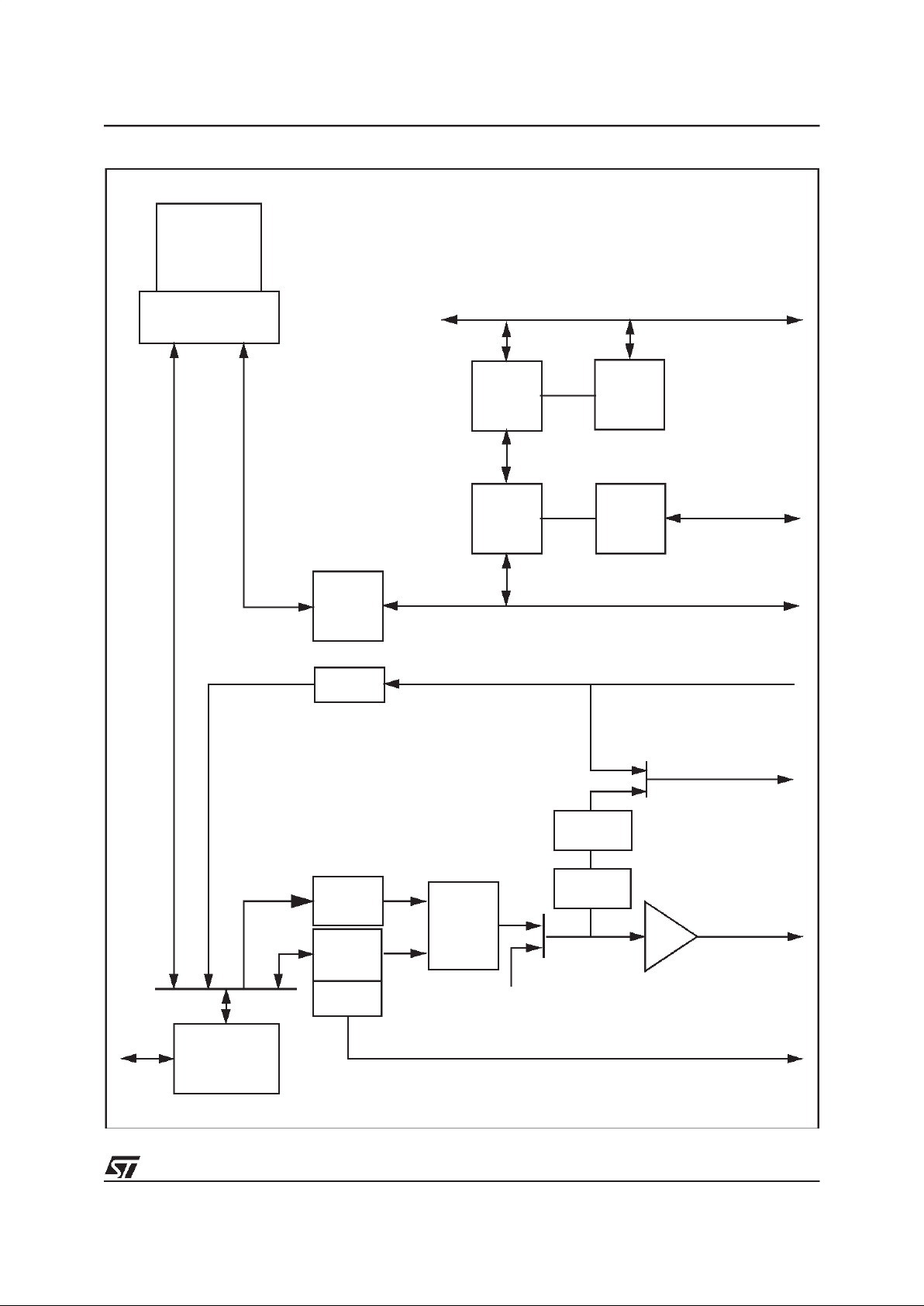
Figure 1-1. Functional description.
x86
Core
Host I/F
DRAM
2D
SVGA
VIP
PCI m/s
PCI BUS
CRTC
HW Cursor
Monitor
TV Output
SYNC Output
Anti-Flicker
Colour Space
Colour
Key
Chroma
Video
pipeline
CCIR Input
ISA
EIDE
PCI m/s
ISA BUS
IPC
EIDE
GENERAL DESCRIPTION
10/48 Issue 1.7 - February 8, 2000
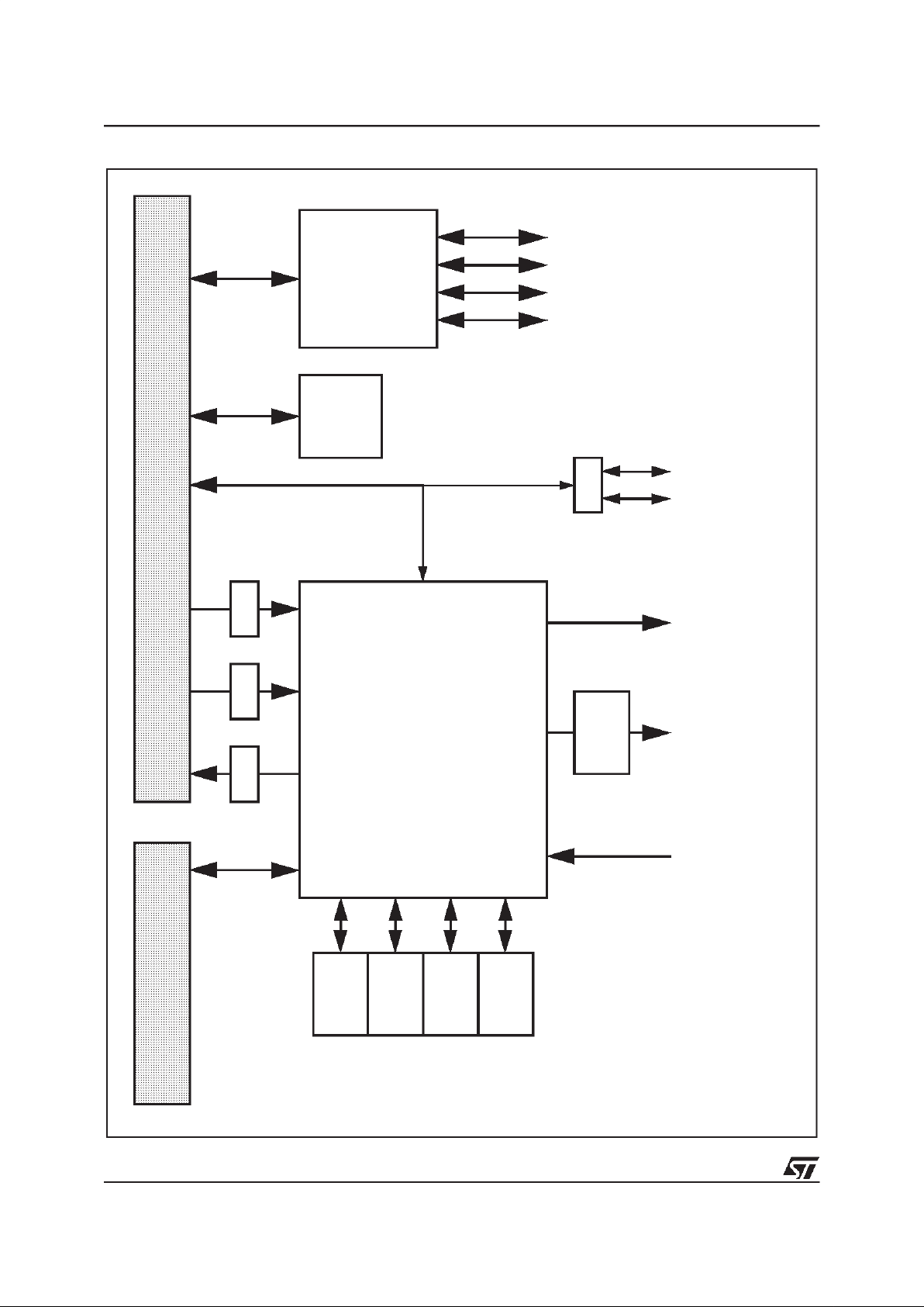
Figure 1-2. Pictorial Block Diagram Typical Application
STPC Client
ISA
PCI
4x 16-bit EDO DRAMs
Super I/O
2x EIDE
Flash
Keyboard / Mouse
Serial Ports
Parallel Port
Floppy
Monitor
TV
STV0119
Video
SVGA
CCIR601
CCIR656
S-VHS
RGB
PAL
NTSC
IRQ
DMA.REQ
DMA.ACK
DMUX
DMUX
MUX
MUX
RTC

PIN DESCRIPTION
Issue 1.7 - February 8, 2000 11/48
2.PIN DESCRIPTION
2.1. INTRODUCTION
The STPC Client integrates most of the functionalities of the PC architecture. As a result, many of
the traditional interconnections between the host
PC microprocessor and the peripheral devices are
totally assimilated to the STPC Client. This offers
improved performance due to the tight coupling of
the processor core and its peripherals. As a result
many of the external pin connections are made directly to the on-chip peripheral functions.
Figure 2-1 shows the STPC Client’s external interfaces. It defines the main busses and their function. Table 2-1 describes the physical implementation listing signals type and their functionality. Table 2-2 provides afull pin listing and description of
the pins. Table 2-3 provides a full listing of pin locations of the STPC Client package by physical
connection. Please refer to the pin allocation
drawing for reference.
Note: Several interface pins are multiplexed with
other functions, refer to the Pin Description section for further details
Table 2-1. Signal Description
Group name Qty
Basic Clocks reset & Xtal (SYS) 14
Memory Interface (DRAM) 89
PCI interface (excluding VDD5) 54
ISA / IDE / IPC combined interface 83
Video Input (VIP) 9
TV Output (TV) 10
VGA Monitor interface (VGA) 10
Grounds 69
V
DD
26
Analog specific V
CC/VDD
14
Reserved/Test/ Misc./ Speaker 10
Total Pin Count 388
Figure 2-1. STPC Client External Interfaces
SOUTHNORTH PCI
X86
DRAM VGA VIP TV SYS ISA/IDE IPC
89 10 9 10 54
14
73 10
STPC CLIENT
PIN DESCRIPTION
12/48 Issue 1.7 - February 8, 2000
Table 2-2. Definition of Signal Pins
Signal Name Dir Description Qty
BASIC CLOCKS RESETS & XTAL
SYSRSTI# I System Reset / Power good 1
SYSRSTO#* O Reset Output to System 1
XTALI I 14.3MHz External Oscillator Input 1
XTALO I/O 14.3MHz External Oscillator Input 1
PCI_CLKI I 33MHz PCI Input Clock 1
PCI_CLKO O 33MHz PCI Output Clock (from internal PLL) 1
ISA_CLK O ISA Clock Output - Multiplexer Select Line For IPC 1
ISA_CLK2X O ISA Clock x 2 Output - Multiplexer Select Line For IPC 1
OSC14M* O ISA bus synchronisation clock 1
HCLK* O Host Clock (Test) 1
DEV_CLK O 24MHz Peripheral Clock (floppy drive) 1
GCLK2X* I/O 80MHz Graphics Clock 1
DCLK* I/O 135MHz Dot Clock 1
DCLK _DIR* I Dot Clock Direction 1
V
DD
_xxx_PLL Power Supply for PLL Clocks
MEMORY INTERFACE
MA[11:0]* I/O Memory Address 12
RAS#[3:0] O Row Address Strobe 4
CAS#[7:0] O Column Address Strobe 8
MWE# O Write Enable 1
MD[63:0]* I/O Memory Data 64
PCI INTERFACE
AD[31:0]* I/O PCI Address / Data 32
CBE[3:0]* I/O Bus Commands / Byte Enables 4
FRAME#* I/O Cycle Frame 1
TRDY#* I/O Target Ready 1
IRDY#* I/O Initiator Ready 1
STOP#* I/O Stop Transaction 1
DEVSEL#* I/O Device Select 1
PAR* I/O Parity Signal Transactions 1
SERR#* O System Error 1
LOCK# I PCI Lock 1
PCI_REQ#[2:0]* I PCI Request 3
PCI_GNT#[2:0]* O PCI Grant 3
PCI_INT[3:0]* I PCI Interrupt Request 4
VDD5 I 5V Power Supply for PCI ESD protection 4
ISA AND IDE COMBINED ADDRESS/DATA
LA[23:22]*/ SCS3#,SCS1# I/O Unlatched Address (ISA) / Secondary Chip Select (IDE) 2
LA[21:20]*/ PCS3#,PCS1# I/O Unlatched Address (ISA) / Primary Chip Select (IDE) 2
LA[19:17]*/ DA[2:0] O Unlatched Address (ISA) / Address (IDE) 3
RMRTCCS#* / DD[15] I/O ROM/RTC Chip Select / Data Bus bit 15 (IDE) 1
KBCS#* / DD[14] I/O Keyboard Chip Select / Data Bus bit 14 (IDE) 1
Note; * denotes theat the pin is V5T(see Section 4. )
PIN DESCRIPTION
Issue 1.7 - February 8, 2000 13/48
RTCRW#* / DD[13] I/O RTC Read/Write / Data Bus bit 13 (IDE) 1
RTCDS#* / DD[12] I/O RTC Data Strobe / Data Bus bit 12 (IDE) 1
SA[19:8]* / DD[11:0] I/O Latched Address (ISA) / Data Bus (IDE) 16
SA[7:0] I/O Latched Address (IDE) 4
SD[15:0]* I/O Data Bus (ISA) 16
ISA/IDE COMBINED CONTROL
IOCHRDY* / DIORDY I/O I/O Channel Ready (ISA) - Busy/Ready (IDE) 1
ISA CONTROL
ALE* O Address Latch Enable 1
BHE#* I/O System Bus High Enable 1
MEMR#*, MEMW#* I/O Memory Read and Memory Write 2
SMEMR#*, SMEMW#* O System Memory Read and Memory Write 2
IOR#*, IOW#* I/O I/O Read and Write 2
MASTER#* I Add On Card Owns Bus 1
MCS16#*, IOCS16#* I Memory/IO Chip Select16 2
REF#* O Refresh Cycle. 1
AEN* O Address Enable 1
IOCHCK#* I I/O Channel Check. 1
ISAOE#* O Bidirectional OE Control 1
GPIOCS#* I/O General Purpose Chip Select 1
IDE CONTROL
PIRQ* I Primary Interrupt Request 1
SIRQ* I Secondary Interrupt Request 1
PDRQ* I Primary DMA Request 1
SDRQ* I Secondary DMA Request 1
PDACK#* O Primary DMA Acknowledge 1
SDACK#* O Secondary DMA Acknowledge 1
PIOR#* I/O Primary I/O Read 1
PIOW#* O Primary I/O Write 1
SIOR#* I/O Secondary I/O Read 1
SIOW#* O Secondary I/O Write 1
IPC
IRQ_MUX[3:0]* I Multiplexed Interrupt Request 4
DREQ_MUX[1:0]* I Multiplexed DMA Request 2
DACK_ENC[2:0]* O DMA Acknowledge 3
TC* O ISA Terminal Count 1
MONITOR INTERFACE
RED, GREEN, BLUE O Red, Green, Blue 3
VSYNC* O Vertical Synchronization 1
HSYNC* O Horizontal Synchronization 1
VREF_DAC I DAC Voltage reference 1
RSET I Resistor Set 1
COMP I Compensation 1
SCL / D DC[1]* I/O I C Interfa ce - Clock / Can be used fo r VGA DDC[1] s ignal 1
Table 2-2. Definition of Signal Pins
Signal Name Dir Descripti on Qty
Note; * denotes theat the pin is V5T(see Section 4. )

PIN DESCRIPTION
14/48 Issue 1.7 - February 8, 2000
SDA / DDC[0 ]* I/O I C Interfa ce - Data / Can be used fo r VG A DDC[0] signal 1
VIDEO INPUT
VCLK* I Pixel Clock 1
VIN[7:0 ]* I YUV Video Da ta Input CCIR 601 or 656 8
DIGITAL TV OUTPUT
TV_YUV [7:0] * O Digital Video Output s 8
ODD_EVEN* O Frame Sy nchronisation 1
VCS* O Hor izontal Line Synchronisation 1
MISCEL LANE OUS
ST[6:0] I/O Test/Misc. pins 7
CLKDEL[2:0]* I/O Reserved (Test/Misc pins) 3
Table 2-2. Definition of Signal Pins
Signal Name Dir Descripti on Qty
Note; * denotes theat the pin is V5T(see Section 4. )

PIN DESCRIPTION
Issue 1.7 - February 8, 2000 15/48
2.2.SIGNAL DESCRIPTIONS
2.2.1. BASIC CLOCKS RESETS & XTAL
PWGD
System Reset/Power good.
This input is
low when the reset switch is depressed. Otherwise, it reflects the power supply’s power good
signal. PWGD is asynchronous to all clocks, and
acts as a negative active reset. The reset circuit
initiates a hard reset on the rising edge of PWGD.
XTALI
14.3MHz Pull Down (10 kΩ)
XTALO
14.3MHz External Oscillator Input
These
pins are the 14.318 MHz external oscillator input;
This clock is used as thereference clock for the internal frequency synthesizer to generate the
HCLK, CLK24M, GCLK2X and DCLK clocks.
HCLK
Host Clock.
This is the host 1X clock. Its
frequency can vary from 25 to 75 MHz. All host
transactions and PCI transactions are synchronized to this clock. This clock drives the DRAM
controller to execute the host transactions. In normal mode, this output clock is generated by the internal PLL.
GCLK2X
80MHz Graphics Clock.
This is the
Graphics 2X clock, which drives the graphics engine and the DRAM controller to execute the
graphics and display cycles.
Normally GCLK2X is generated by the internal frequency synthesizer, and this pin is an output. By
setting a bit in Strap Register 2, this pin can be
made an input so that an external clock can replace the internal frequency synthesizer.
DCLK
135MHz Dot Clock.
This is the dot clock,
which drivesgraphicsdisplay cycles. Its frequency
can go from 8MHz (using internal PLL) up to 135
MHz, and it is required to have a worst case duty
cycle of 60-40.
DCLK_DIR
Dot ClockDirection.
Specifies if DCLK
is an input (0) or an output (1).
DEV_CLK
24MHz Peripheral Clock Output.
This
24MHZ signal is provided as a convenience for
the system integration of a floppy disk driver function in an external chip.
2.2.2. MEMORY INTERFACE
MA[11:0]
Memory Address Output.
These 12 multiplexed memory address pins support external
DRAM with up to 4K refresh. These include all
16M x N and some 4M x N DRAM modules. The
address signals must be externally buffered to
support more than 16 DRAM chips. The timing of
these signals can be adjusted by software to
match the timings of most DRAM modules.
MD[63:0]
Memory Data I/O.
This is the 64-bit
memory data bus. If only half of a bank is populated, MD63-32 is pulled high, data is on MD31-0.
MD[40-0] are read by the device strap option registers during rising edge of PWGD.
RAS#[3:0]
Row Address Strobe Output.
There
are 4 active low row address strobe outputs, one
for each bank of the memory. Each bank contains
4 or 8-Bytes of data. The memorycontroller allows
half of a bank (4 Bytes) to be populated to enable
memory upgrade at finer granularity.
The RAS# signals drive the SIMMs directly without any external buffering. These pins are always
outputs, but they can also simultaneously be inputs, to allow the memory controller to monitor the
value of the RAS# signals at the pins.
CAS#[7:0]
Column AddressStrobe Output.
There
are 8 active low column address strobe outputs,
one for each Byte of the memory.
The CAS# signals drive the SIMMs either directly
or through external buffers.
These pins are always outputs, but they can also
simultaneously be inputs, to allow the memory
controller to monitor the value of the CAS# signals
at the pins.
MWE#
Write Enable Output.
Write enable specifies whether the memory access is a read (MWE#
= H) or a write (MWE# = L). This single write enable controls all DRAMs. It can be externally buffered to boost the maximum number of loads
(DRAM chips) supported.
The MWE# signals drive the SIMMs directly without any external buffering.
2.2.3. VIDEO INPUT
VCLK
Pixel Clock Input.
VIN[7:0]
YUV Video Data Input CCIR 601 or 656.
Time multiplexed 4:2:2 luminance and chrominance data as defined in ITU-R Rec601-2 and
Rec656 (except for TTL input levels). This bus interfaces with an MPEG video decoder output port
and typically carries a stream ofCb, Y, Cr, Y digital video at VCLK frequency, clocked on the rising
edge (by default) of VCLK. A 54-Mbit/s ‘double’
Cb, Y, Cr, Y input multiplex is supported for double
encoding applications (rising and falling edge of
CKREF are operating).
2.2.4. TV OUTPUT
TV_YUV[7:0]
Digital video outputs.
 Loading...