

SGS Thomson Microelectronics STPCC03 Datasheet
STPC CONSUMER-S
PC Compatible Embeded Microprocessor
ADVANCED DATA
1/5129/10/99
Release B
This is preliminary information on a new product now in development or undergoing evaluation. Details are subject to change without notice.
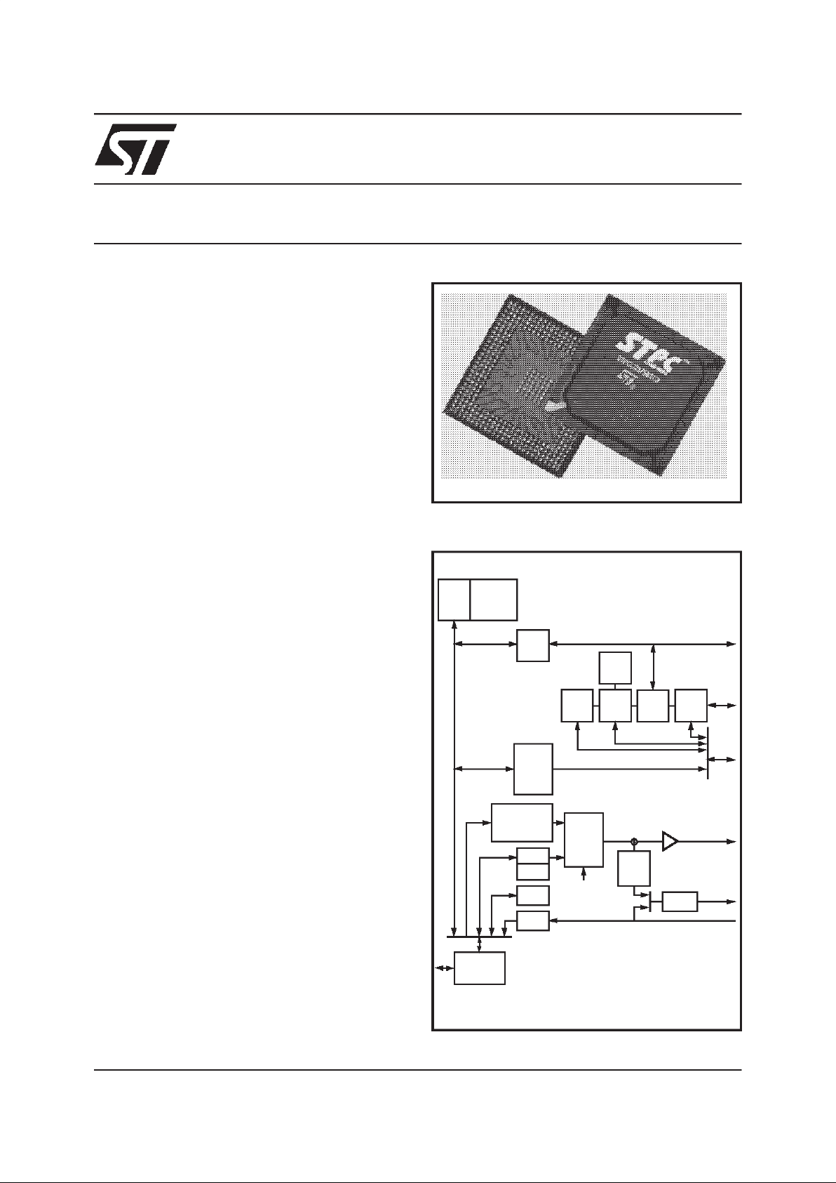
Figure 1. Logic Diagram
■ POWERFUL x86 PROCESSOR
■ 64-BIT 66MHz SDRAM UMA CONTROLLER
■ VGA & SVGA CRT CONTROLLER
■ 2D GRAPHICS ENGINE
■ VIDEO INPUT PORT
■ VIDEO PIPELINE
- UP-SCALER
- VIDEO COLOR SPACE CONVERTER
- CHROMA & COLOUR KEY SUPPORT
■ TV OUTPUT
- 3-LINE FLICKER FILTER
- CCIR 601/656 SCAN CONVERTER
- NTSC / PAL COMPOSITE, RGB, S-VIDEO
■ PCI MASTER / SLAVE CONTROLLER
■ ISA MASTER / SLAVE CONTROLLER
■ INTEGRATED PERIPHERAL CONTROLLER
- DMA CONTROLLER
- INTERRUPT CONTROLLER
- TIMER / COUNTERS
■ OPTIONAL 16-BIT LOCAL BUSINTERFACE
■ EIDE CONTROLLER
■ I C INTERFACE
■ POWER MANAGEMENT UNIT
■ 3.3V OPERATION
STPC CONSUMER-S OVERVIEW
The STPC Consumer-S integrates a standard 5th
generation x86 core, a Synchronous DRAM controller, a graphics subsystem, a video input port,
video pipeline, and support logic i ncluding PCI,
ISA, and IDE controllers to provide a s ingle consumer orientated PC compatible subsystem on a
single device.
The device is based on a tightly coupled U nified
Memory Architecture (UMA), sharing the same
memory array between the CPU main memory
and the graphics and video frame buffers.
The STPC Consumer-S is packaged in a 388
Plastic Ball Grid Array (PBGA).
PBGA3 88
x86
Core
Host
I/F
SDRAM
CTRL
SVGA
GE
VIP
PCI
m/s
LB
CTR
PCI Bus
ISA
m/s
IPC
PCI
m/s
ISA Bus
CRTC
Cursor
Moni tor
TV
IDE
I/F
PMU
W.dog
Video
Pipeline
C Key
K Key
LUT
Local Bus
Encoder
TVO

STPC CONSUMER-S
2/51
Release B
This is preliminary information on a new product now in development or undergoing evaluation. Details are subject to change without notice.
■ X86 Processor core
■ Fully static 32-bit 5-stage pipeline, x86
processor fully PC compatible.
■ Can access up to 4GB of external memory.
■ 8Kbyte unified instruction and data cache
with write back and write through capability.
■ Parallelprocessing integral floating pointunit,
with automatic power down.
■ Fully static design for dynamic clock control.
■ Low power and system management modes.
■ SDRAM Controller
■ 64-bit data bus.
■ Up to 66MHz SDRAM clock speed.
■ Integrated system memory, graphic frame
memory and video frame memory.
■ Supports 2MB up to 128 MB memory.
■ Supports 8MB, 16M, and 32MB DIMMs.
■ Supports buffered, non buffered,and
registered DIMMs
■ 4-line write buffersfor CPUto DRAM and PCI
to DRAM cycles.
■ 4-line read prefetch buffers for PCI masters.
■ Programmable latency
■ Programmable timing for DRAM parameters.
■ Supports -8, -10, -12, -13, -15 memory parts
■ Supports 1MB up to 8MB memory hole.
■ 32-bit accesses not supported.
■ Autoprecharge not supported.
■ Power down not supported.
■ FPM and EDO not supported.
■ Graphics Controller
■ 64-bit windows accelerator.
■ Compatibility to VGA & SVGA standards.
■ Hardware acceleration for text, bitblts,
transparent blts and fills.
■ Up to 64 x 64 bit graphics hardware cursor.
■ Up to 4MB long linear frame buffer.
■ 8-, 16-, and 24-bit pixels.
■ CRT Controller
■ Integrated 135MHz triple RAMDAC allowing
for 1024 x 768 x 75Hz display.
■ 8-, 16-, 24-bit pixels.
■ Interlaced or non-interlaced output.
■ Video Input port
■ Accepts video inputs in CCIR 601 mode.
■ Optional 2:1 decimator
■ Stores captured video in off setting area of
the onboard frame buffer.
■ Video pass through to the onchip PAL/NTSC
encoder for full screen video images.
■ HSYNC and B/T generation or lock onto
external video timing source.
■ Video Pipeline
■ Two-tapinterpolative horizontal filter.
■ Two-tapinterpolative vertical filter.
■ Color space conversion.
■ Programmable window size.
■ Chroma and color keying for integrated video
overlay.
■ TV Output
■ Programmable two tap filter with gamma
correction or three tap flicker filter.
■ Progressiveto interlaced scan converter.
■ NTSC-M, PAL-M,PAL-B,D,G,H,I,PAL-N easy
programmable video outputs.
■ CCIR601 encoding with programmable color
subcarrier frequencies.
■ Line skip/insert capability
■ Interlaced or non-interlaced operation mode.
■ 625 lines/50Hz or 525 lines/60Hz 8 bit
multiplexedCB-Y-CR digital input.
■ CVBS and R,G,B simultaneous analog
outputs through 10-bit DACs.
■ Cross color reductionby specific trap filtering
on luma within CVBS flow.
■ Power down mode available on each DAC.

STPC CONSUMER-S
3/51
Release B
This is preliminary information on a new product now in development or undergoing evaluation. Details are subject to change without notice.
■ PCI Controller
■ Fully compliant with PCI 2.1 specification.
■ Integrated PCI arbitration interface. Up to 3
masters can connect directly. External PAL
allows forgreater than 3masters.
■ Translation of PCI cycles to ISA bus.
■ Translation of ISA master initiated cycle to
PCI.
■ Support forburst read/write from PCI master.
■ PCI clock is 1/3 or 1/2 Host clock .
■ ISA master/slave controller
■ Generates the ISA clock from either
14.318MHz oscillator clock or PCI clock
■ Supports programmable extrawait state for
ISA cycles
■ Supports I/O recovery time for back to back I/
O cycles.
■ Fast Gate A20 and Fast reset.
■ Supports the single ROM that C, D,or E.
blocks shares with F blockBIOS ROM.
■ Supports flash ROM.
■ Supports ISA hidden refresh.
■ Buffered DMA &ISA master cycles to reduce
bandwidth utilization of thePCI andHost bus.
NSP compliant.
■ Integrated Peripheral Controller
■ 2X8237/AT compatible 7-channel DMA
controller.
■ 2X8259/AT compatible interrupt Controller.
16 interrupt inputs - ISAand PCI.
■ Three 8254 compatible Timer/Counters.
■ Co-processor error support logic.
■ Supports external RTC.
■ Local Bus interface
■ Multiplxed with ISA interface.
■ Low latency bus
■ 22-bit address bus.
■ 16-bit data bus with word steering capability.
■ Programmable timing (Host clockgranularity)
■ 2 Programmable Flash Chip Select.
■ 5 Programmable I/O Chip Select.
■ Supports 32-bit Flashburst.
■ 2-level hardwarekeyprotection forFlash boot
block protection.
■ Supports 2 banksof 8MB flash devices with
boot block shadowed to 0x000F0000.
■ IDE Interface
■ Supports PIO and Bus Master IDE
■ Supports up to Mode 5 Timings
■ Transfer Rates to 22 MBytes/sec
■ Supports up to 4 IDE devices
■ Concurrent channel operation (PIO & DMA
modes) - 4 x 32-Bit Buffer FIFO per channel
■ Support for PIO mode 3 & 4.
■ Support for DMA mode 1 & 2.
■ Support for 11.1/16.6 MB/s,I/O Channel
Ready PIO data transfers.
■ Supports 13.3/16.6 MB/s DMA data transfers
■ Bus Master with scatter/gather capability
■ Multi-word DMA support for fast IDE drives
■ Individual drive timing for all four IDEdevices
■ Supports both legacy & native IDE modes
■ Supports hard drives larger than 528MB
■ Support for CD-ROM and tape peripherals
■ Backward compatibilitywith IDE (ATA-1).
■ Power Management
■ Four powersaving modes: On, Doze,
Standby, Suspend.
■ Programmable system activity detector
■ Supports SMM.
■ Supports STOPCLK.
■ Supports IO trap & restart.
■ Independent peripheral time-out timer to
monitor hard disk, serial & parallel ports.
■ Supports RTC,interrupts and DMAs wake-up

GENERAL DESCRIPTION
4/51
Release B
This is preliminary information on a new product now in development or undergoing evaluation. Details are subject to change without notice.
1 GENERAL DESCRIPTION
At the heart of the STPC Consumer-S is an advanced 64-bit processor block, dubbed the
5ST86. The 5ST86 includes a 486 processor core
along with a 64-bit SDRAM controller, advanced
64-bit accelerated graphics and video controller, a
high speed PCI local-bus controller and Industry
standard PC chip set functions (Interrupt controller, DMA Controller, Interval timer and ISA bus).
The STPC Consumer-S makes use of a tightly
coupled Unified Memory Architecture (UMA),
where the same memory array is used for CPU
main memory and graphics frame-buffer. This
means areduction in total system memoryfor system performances that are equal to that of a comparable frame buffer and system memory based
system, and generally much better, due to the
higher memory bandwidth allowed by attaching
the graphics engine directly to the 64-bit processor hostinterface runningat the speed of theprocessor bus rather than the traditional PCI bus.
The 64-bit wide memory array provides the system with 528MB/speak bandwidth. This allowsfor
higher resolution screens andgreater color depth.
The ‘standard’ PC chipset functions (DMA, interrupt controller, timers, power management logic)
are integrated together with the x86 processor
core; additional functions such as communications ports are accessed by the STPC ConsumerS via internal ISA bus.
The PCI bus is the main data communication link
to the STPC Consumer-S chip. The STPC Consumer-S translates appropriate host bus I/O and
Memory cycles onto the PCI bus. It also supports
generation ofConfiguration cycles on the PCI bus.
The STPC Consumer-S, as a PCI bus agent (host
bridge class), fully complies with PCI specification
2.1. The chip-set also implements the PCI mandatory header registers in Type 0 PCI configuration
space for easy porting of PCI aware system BIOS. The devicecontains a PCI arbitration function
for three external PCI devices.
The STPC Consumer-S has two functionnal
blocks
sharing the same balls
: The ISA / IPC /
IDE block and the Local Bus / IDE block (see Table 3). Any board with the STPC Consumer-S
should be built usingonly oneof these two configurations.
At reset, the configuration is done by ‘strap options’ which initialises the STPC Consumer-S to
the right settings. It is a set of pull-up or pull-down
resistors on the memory data bus, checked on reset, which auto-configure theSTPC Consumer-S.
GRAPHICS FUNCTIONS
Graphics functions are controlled through the onchip SVGA controller and the monitor display is
produced through the 2D graphics display engine.
This Graphics Engine is tuned to work with the
host CPU to provide a balanced graphics system
with a low silicon area cost. It performs limited
graphics drawing operations which include hardware acceleration of text, bitblts, transparent blts
and fills. The results of these operations change
the contents of the on-screen or off-screen frame
buffer areas of DRAM memory. The frame buffer
can occupy a space up to 4 Mbytes anywhere in
the physical main memory and always starts from
the bottom of the main physical memory.
The graphics resolution supported is a maximum
of 1280x1024 in 65536 colours and 1024x768 in
true color at 75Hz refresh rate and is VGA and
SVGA compatible. Horizontal timing fields are
VGA compatible while the vertical fields are extended by one bit to accommodate above display
resolution.
VIDEO FUNCTIONS
The STPC Consumer-S provides several additional functions to handle MPEG or similar video
streams. The Video Input Port accepts an encoded digital video stream in one of a number of industry standard formats, decodes it, optionally
decimates it, and deposits it into an off screen
area of the frame buffer. An interrupt request can
be generated when an entire field or frame has
been captured. The video output pipeline incorporates a video-scaler and color space converter
function and provisions in the CRT controller to
display a video window. While repainting the
screen the CRT controller fetches both the video
as well as the normal non-video frame buffer in
two separate internal FIFOs. The video stream
can be color-space converted (optionally) and
smooth scaled. Smooth interpolative scaling in
both horizontal and vertical direction are implemented. Color and Chroma key functions are also
implemented to allow mixing video stream with
non-video frame buffer.
The video output passes directly to the RAMDAC
for monitor output or through another optional
color spaceconverter (RGBto 4:2:2 YCrCb) to the
programmable anti-flicker filter. The flicker filter is
configured as either a two line filter with gamma
correction (primarily designed for DOS type text)
or a 3 line flicker filter (primarily designed for Windows type displays). Thefliker filter is optional and
can besoftware disabled foruse with large screen
area’s of video.

GENERAL DESCRIPTION
5/51
Release B
This is preliminary information on a new product now in development or undergoing evaluation. Details are subject to change without notice.
The Video output pipeline of the STPC ConsumerS interfaces directly to the internal digital TV encoder. It takes a 24 bit RGB non-interlaced pixel
stream and converts to a multiplexed 4:2:2 YCrCb
8 bit output stream, the logic includes a progressive to interlaced scan converter and logic to insert appropriate CCIR656 timing reference codes
into the outputstream. It facilitates the high quality
display of VGA or full screen video streams received via the Video input port to standard NTSC
or PAL televisions.
The digital PAL/NTSC encoder outputs interlaced
or non-interlaced video in PAL-B,D,G,H,I PAL-N,
PAL-M or NTSC-Mstandards and “NTSC- 4.43” is
also possible.
The four frame (for PAL) or 2 frame (for NTSC)
burst sequences are internally generated, subcarrier generation being performed numerically with
CKREF as reference. Rise and fall times of synchronisation tips and burst envelope are internally
controlled according to the relevant ITU-R and
SMPTE recommendations.
Video output signals are directed to four analog
output pins through internal D/A convertersgiving,
simultaneous R,G,B and composite CVBS outputs.
IDE INTERFACE
An industry standard EIDE (ATA 2) controller is
built into the STPC Consumer-S. The IDE port is
capable of supporting a total of four devices.
POWER MANAGEMENT
The STPC Consumer-Score is compliantwith the
Advanced Power Management (APM) specification to provide a standard method by which the
BIOS can control the power used by personal
computers. The Power Management Unit module
(PMU) controls the power consumption providing
a comprehensive set of features that control the
power usage and supports compliance with the
United States Environmental Protection Agency’s
Energy Star Computer Program. The PMU provides following hardware structures to assist the
software in managing the power consumption by
the system.
- System Activity Detection.
- Three power down timers.
- Doze timer for detecting lack of system activity
for short durations.
- Stand-by timer for detecting lack of system activity for medium durations
- Suspend timer for detectinglack of system activity for long durations.
- House-keeping activity detection.
- House-keeping timerto cope with short bursts of
house-keeping activity while dozing or in stand-by
state.
- Peripheral activity detection.
- Peripheral timer for detecting lack of peripheral
activity
- SUSP# modulation to adjust the system performance in various power down states of the system
including full power on state.
- Power control outputs to disable power from different planes of the board.
Lack of system activity for progressively longer
period of times is detected by the three power
down timers. These timers can generate SMI interrupts to CPU so that the SMM software can put
the system in decreasing states of power consumption. Alternatively, system activity in apower
down statecan generateSMI interrupt toallow the
software to bring the system back up to full power
on state. The chip-set supports up to three power
down states: Doze state, Stand-by state and Suspend mode. These correspond to decreasing levels of power savings.
POWER DOWN
Power downputs theSTPC Consumer-S into suspend mode. The processor completes execution
of thecurrent instruction, any pending decoded instructions and associated bus cycles. During the
suspend mode, internal clocks are stopped. Removing power down, the processor resumes instruction fetching and begins execution in the instruction stream at the point it had stopped. Because of the static nature of the core, no internal
data is lost.

GENERAL DESCRIPTION
6/51
Release B
This is preliminary information on a new product now in development or undergoing evaluation. Details are subject to change without notice.
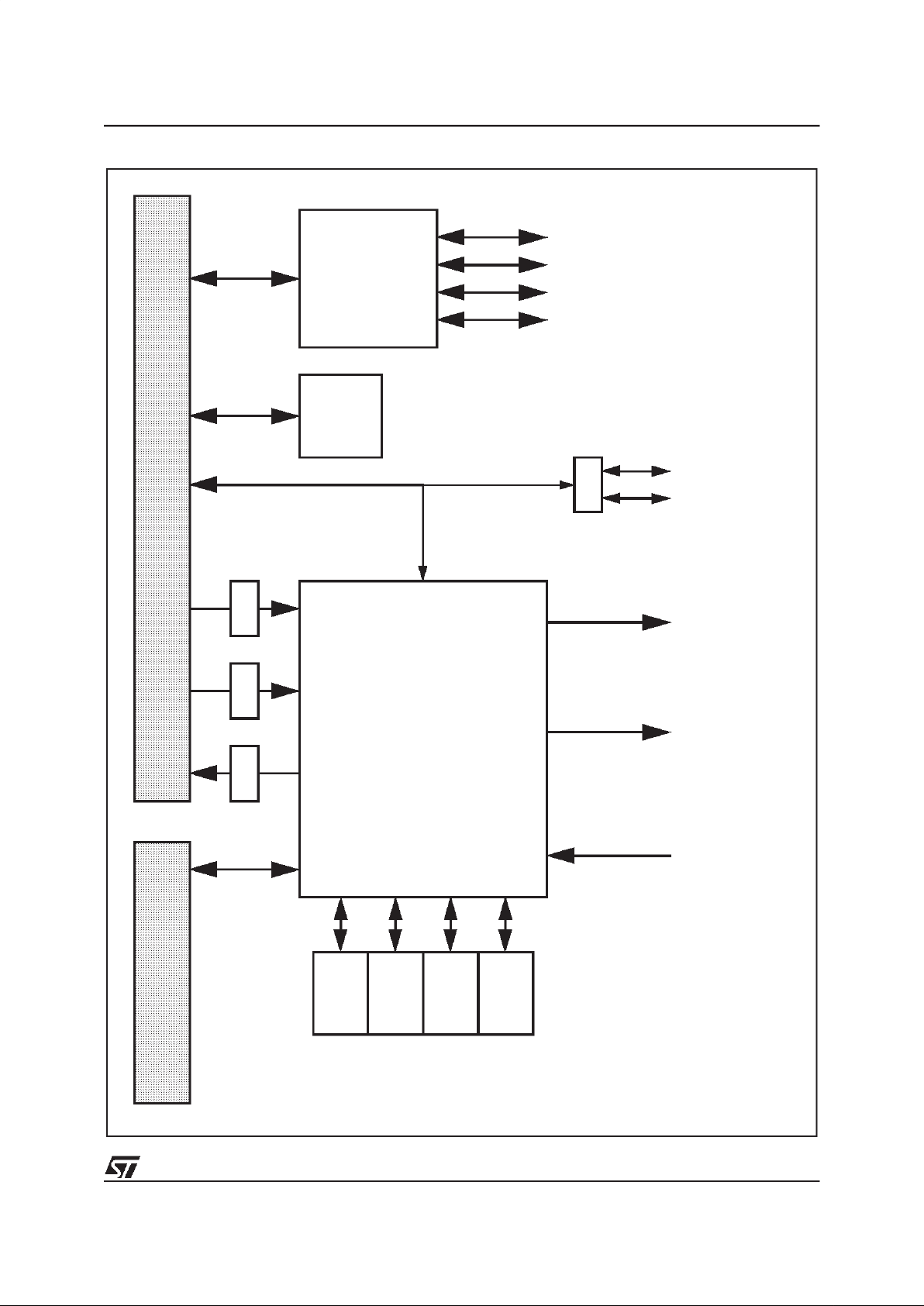
Figure 2. Functionnal description.
x86
Core
Host
I/F
SDRAM
I/F
SVGA
GE
VIP
PCI m/s
Local
Bus I/F
PCI BUS
ISA
m/s
IPC
82C206
PCI m/s
ISA Bus
CRTC
HW Cursor
Monitor
TV
- Pixel formating
- Scaler
- Colour Space
IDE
I/F
PMU
watch-
Video Pipeline
Colour Key
Chroma Key
LUT
Local Bus
NTSC/PAL
Encoder
TVO
- CSC
-FF
- CCIR
CCIR Input
GENERAL DESCRIPTION
7/51
Release B
This is preliminary information on a new product now in development or undergoing evaluation. Details are subject to change without notice.
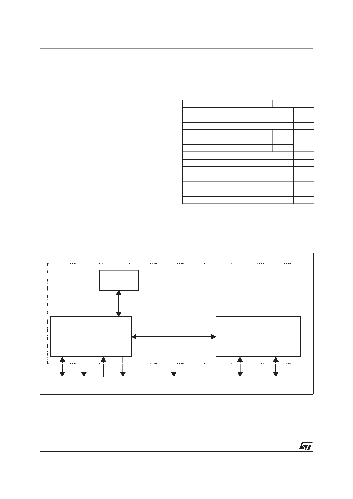
Figure 3. Typical Application
STPC Consumer-S
ISA
PCI
4x 16-bit SDRAMs
Super I/O
2x EIDE
Flash
Keyboard / Mouse
Serial Ports
Parallel Port
Floppy
Monitor
TV
Video
SVGA
CCIR601
CCIR656
S-VHS
RGB
PAL
NTSC
IRQ
DMA.REQ
DMA.ACK
DMUX
DMUX
MUX
MUX
RTC

GENERAL DESCRIPTION
8/51
Release B
This is preliminary information on a new product now in development or undergoing evaluation. Details are subject to change without notice.

Update History for Video controller chapter
9/51
Release B
1.1 UPDATE HISTORY FOR VIDEO CONTROLLER CHAPTER
The following changes have been made to the General Description Chapter on 29/10/99.
Section Change Text
1 Removed
“The STPC Consumer-S has in addition to the 5ST86 a TFT output, a Local
Bus interface, a WatchDog and a JTAG interface.”
PIN DESCRIPTION
10/51
Release B
This is preliminary information on a new product now in development or undergoing evaluation. Details are subject to change without notice.
2 PIN DESCRIPTION
2.1 INTRODUCTION
The STPC Consumer-S integrates most of the
functionalities of the PC architecture. As a result,
many of the traditional interconnections between
the host PC microprocessor and the peripheral
devices are totally internal to the STPC Consumer-S. This offers improved performance due to the
tight coupling of the processor core and these peripherals. As aresult many of the externalpin connections are madedirectlyto the on-chipperipheral functions.
Figure 2.1 shows the STPC Consumer-S external
interfaces. It defines the main busses and their
function. Table 2.1 describes the physical implementation listing signals type and their functionality. Table 2.2 provides a full pin listing and description of pins. Table 2.5 provides a full listing of pin
locations of the STPC Consumer-S package by
physical connection.
Note: Several interface pins are multiplexed with
other functions, refer to Table 2.3 and Table 2.4
for further details
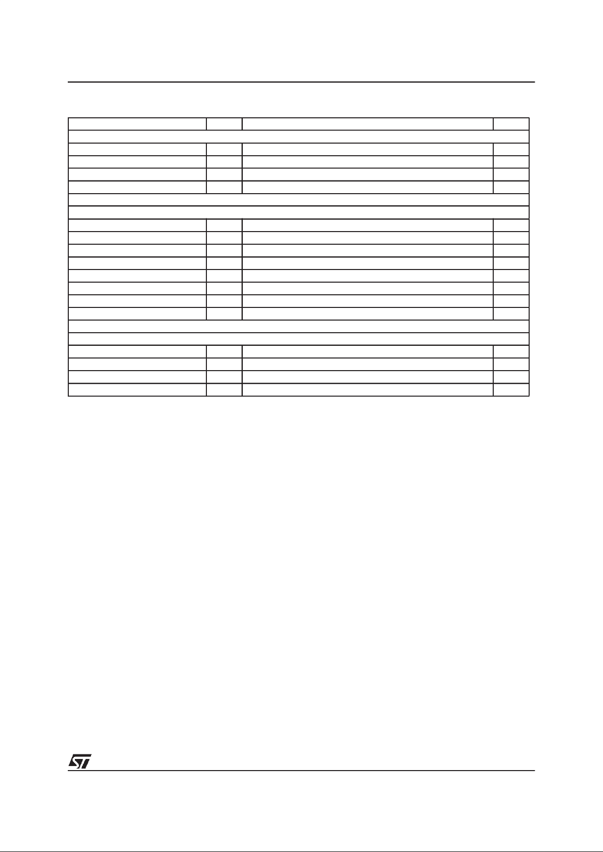
Table 2.1. Signal Description
Group name Qty
System Clocks & Resets 11
Memory Interface 95
PCI interface 60
ISA 79
89IDE 34
Local Bus 49
Video Input 11
TV Output 8
VGA Monitor interface 8
Grounds 71
V
DD
29
Analog specific V
CC/VDD
6
Total Pin Count 388
Figure 2.1. STPC Consumer-S External Interfaces
PCI
x86
SDRAM VGA VIP TV SYS ISA/IDE/LB
95 8 11 8 60 11 89
STPC CONSUMER-S

PIN DESCRIPTION
11/51
Release B
This is preliminary information on a new product now in development or undergoing evaluation. Details are subject to change without notice.
Table 2.2. Definition of Signal Pins
Signal Name Dir Description Qty
BASIC CLOCKS AND RESETS
SYSRSTI# I System Power Good Input 1
SYSRSTO# O System Reset Output 1
XTALI I 14.3MHz Crystal Input 1
XTALO I/O 14.3MHz Crystal Output - External Oscillator Input 1
HCLK I/O Host Clock (Test) 1
DEV_CLK O 24MHz Peripheral Clock (floppy drive) 1
DCLK I/O 27-135MHz Graphics Dot Clock 1
MEMORY INTERFACE
MCLKI I Memory Clock Input 1
MCLKO O Memory Clock Output 1
CS#[3:0] O DIMM Chip Select 4
MA[11:0] O Memory Row & Column Address 12
MD[63:0] I/O Memory Data 64
RAS#[1:0] O Row Address Strobe 2
CAS#[1:0] O Column Address Strobe 2
MWE# O Write Enable 1
DQM[7:0] O Data Input/Output Mask 8
PCI INTERFACE
PCI_CLKI I 33MHz PCI Input Clock 1
PCI_CLKO O 33MHz PCI Output Clock (from internal PLL) 1
AD[31:0] I/O PCI Address / Data 32
CBE#[3:0] I/O Bus Commands / Byte Enables 4
FRAME# I/O Cycle Frame 1
IRDY# I/O Initiator Ready 1
TRDY# I/O Target Ready 1
LOCK# I PCI Lock 1
DEVSEL# I/O Device Select 1
STOP# I/O Stop Transaction 1
PAR I/O Parity Signal Transactions 1
SERR# O System Error 1
PCIREQ#[2:0] I PCI Request 3
PCI_GNT#[2:0] O PCI Grant 3
PCI_INT[3:0] I PCI Interrupt Request 4
VDD5 I 5V Power Supply for PCI ESD protection 4
ISA CONTROL
ISA_CLK O ISA Clock Output - Multiplexer Select Line For IPC 1
ISA_CLK2X O ISA Clock x2 Output - Multiplexer Select Line For IPC 1
OSC14M O ISA bus synchronisation clock 1
LA[23:17] O Unlatched Address 7
SA[19:0] I/O Latched Address 20
SD[15:0] I/O Data Bus 16
ALE O Address Latch Enable 1
MEMR#, MEMW# I/O Memory Read and Memory Write 2
SMEMR#, SMEMW# O System Memory Read and Memory Write 2
PIN DESCRIPTION
12/51
Release B
This is preliminary information on a new product now in development or undergoing evaluation. Details are subject to change without notice.
IOR#, IOW# I/O I/O Read and Write 2
MCS16#, IOCS16# I Memory/IO Chip Select16 2
BHE# O System Bus High Enable 1
ZWS# I Zero Wait State 1
REF# O Refresh Cycle. 1
MASTER# I Add On Card Owns Bus 1
AEN O Address Enable 1
IOCHCK# I I/O Channel Check. 1
IOCHRDY I/O I/O Channel Ready (ISA) - Busy/Ready (IDE) 1
ISAOE# O ISA/IDE Selection 1
GPIOCS# I/O General Purpose Chip Select 1
IRQ_MUX[3:0] I Time-Multiplexed Interrupt Request 4
DREQ_MUX[1:0] I Time-Multiplexed DMA Request 2
DACK_ENC[2:0] O Encoded DMA Acknowledge 3
TC O ISA Terminal Count 1
RTCAS O Real Time Clock Address Strobe 1
RMRTCCS# I/O ROM/RTC Chip Select 1
KBCS# I/O Keyboard Chip Select 1
RTCRW# I/O RTC Read/Write 1
RTCDS I/O RTC Data Strobe 1
LOCAL BUS
PA[21:0] O Address Bus 22
PD[15:0] I/O Data Bus 16
PRD1#,PRD0# O Peripheral Read Control 2
PWR1#,PWR0# O Peripheral Write Control 2
PRDY# I Data Ready 1
FCS1#, FCS0# O Flash Chip Select 2
IOCS#[3:0] O I/O Chip Select 4
IDE CONTROL
DA[2:0] O Address Bus 3
DD[15:0] I/O Data Bus 16
PCS3#,PCS1#,SCS3#,SCS1# O Primary &Secondary Chip Selects 4
DIORDY O Data I/O Ready 1
PIRQ, SIRQ I Primary & Secondary Interrupt Request 2
PDRQ, SDRQ I Primary &Secondary DMA Request 2
PDACK#, SDACK# O Primary &Secondary DMA Acknowledge 2
PDIOR#, SDIOR# O Primary &Secondary I/O Channel Read 2
PDIOW#, SDIOW# O Primary &Secondary I/O Channel Write 2
MONITOR INTERFACE
RED, GREEN, BLUE O Analog Red, Green, Blue 3
VSYNC O Vertical Sync 1
HSYNC O Horizontal Sync 1
VREF_DAC I DAC Voltage reference 1
RSET I Resistor Set 1
COMP I Compensation 1
Table 2.2. Definition of Signal Pins
Signal Name Dir Description Qty
PIN DESCRIPTION
13/51
Release B
This is preliminary information on a new product now in development or undergoing evaluation. Details are subject to change without notice.
2.2 SIGNAL DESCRIPTIONS
2.2.1 BASIC CLOCKS AND RESETS
SYSRSTI#
System Reset/Power good.
This input
is low when the reset switch is depressed. Otherwise, it reflects the power supply’s power good
signal. This input is asynchronous to all clocks,
and acts as anegative active reset. The reset circuit initiates a hard reset on the rising edge of this
signal.
SYSRSTO#
Reset Output to System.
This is the
system reset signaland is usedto reset therest of
the components (not on Host bus) in the system.
The ISA bus reset is an externally inverted buffered version of this outputand thePCI bus reset is
an externally buffered version of this output.
XTALI
14.3MHz Crystal Input
XTALO
14.3MHz Crystal Output.
These pins are
connected to the 14.318 MHz crystal to provide
the reference clock for the internal frequency synthesizer to generate all the other clocks.
A 14.318 MHz Series Cut Crystal should be connected between these two pins. Balance capacitors of 15 pF should alsobe added. In the eventof
an external quarzt oscillator providing the master
clock signal to the STPC Consumer-S device, the
TTL signal should be provided on XTALO.
HCLK
Host Clock.
This clock supplies the CPU
and the host related blocks. This clock can e doubled inside the CPU and is intended to operate in
the range of25 to 100 MHz. Thisclock in generated internally from a PLL but can be driven directly
from the external system.
DCLK
Dot Clock / Pixelclock.
This clock supplies
the display controller, the video pipeline, the ramdac, and the TV output logic. Its value is dependent on the selected display mode.
Its frequencycan be as high as 135MHz. Thissignal is either driven by the internal PLL either byan
external oscillator. The direction can be controlled
by a strap option oran internal register bit.
DEV_CLK
24MHz Peripheral Clock.
This 24MHZ
signal is provided asa convenience for thesystem
integration of a Floppy Disk driver function in an
external chip.
VIDEO INPUT
VCLK I 27-33MHz Video Input Port Clock 1
VIN I CCIR 601 or 656 YUV Video Data Input 8
VCS I/O Composite Synch orHorizontal line SYNC output 1
ODD_EVEN I/O Frame Synchronisation 1
ANALOG TV OUTPUT
RED_TV, GREEN_TV, BLUE_TV O Analog RGB or S-VHS outputs 3
CVBS O Analog video composite output 1
IREF1_TV I Reference current of 9bit DAC for CVBS 1
VREF1_TV I Reference voltage of 9bit DAC for CVBS 1
IREF2_TV I Reference current of 8bit DAC for R,G,B 1
VREF2_TV I Reference voltage of 8bit DAC for R,G,B 1
VSSA_TV I Analog Vss for DAC 1
VDDA_TV I Analog Vdd for DAC 1
MISCELLANEOUS
SPKRD O Speaker Device Output 1
SCL I/O I C Interface - Clock / Can be used for VG A D DC[1] signal 1
SDA I/O I C Interface - Data /Can be used for VGA DDC[0] signal 1
SCAN_ENAB LE I Reserved (Te st pin) 1
Table 2.2. Definition of Signal Pins
Signa l Name Dir Description Qty

PIN DESCRIPTION
14/51
Release B
This is preliminary information on a new product now in development or undergoing evaluation. Details are subject to change without notice.
2.2.2 MEMORY INTERFACE
MCLKO
Memory Clock Output.
This clock is driving the DIMMs on board and is generated from an
internal PLL. The default value is 66MHz.
MCLKI
Memory Clock Input.
This clock is driving
the SDRAM controller, the graphics engine and
display controller. This input should be a buffered
version ofthe MCLKOsignal with the track lengths
between the buffer and the pin matched with the
track lengths between the buffer and the DIMMs.
CS#[3:0]
Chip Select
These signals are used to
disable or enable device operation by masking or
enabling all SDRAM inputs except MCLK, CKE,
and DQM.
MA[11:0]
Memory Address.
Multiplexed row and
column address lines.
MD[63:0]
Memory Data.
This is the 64-bit memory
data bus. MD[40-0] are read by the device strap
option registers during rising edge of SYSRSTI#.
RAS#[1:0]
Row Address Strobe.
These signals
enable row access and precharge. Row address
is latched on rising edge of MCLK when RAS# is
low.
CAS#[1:0]
Column Address Strobe.
These signals enable column access. Column address is
latched on rising edge of MCLK when CAS# is
low.
MWE#
Write Enable.
Write enable specifies
whether thememory accessis a read(MWE# =H)
or a write (MWE# = L).
DQM#[7:0]
Data Mask.
Makes data output Hi-Z
after the clock and masks the SDRAM outputs.
Blocks SDRAM data input when DQM active.
2.2.3 PCI INTERFACE
PCI_CLKI
33MHz PCI Input Clock.
This signal is
the PCI bus clock inputand shouldbe driven from
the PCI_CLKO pin.
PCI_CLKO
33MHz PCI Output Clock.
This is the
master PCI bus clock output.
AD[31:0]
PCI Address/Data.
This is the 32-bit
multiplexed address and databus of the PCI. This
bus is driven by the master during the address
phase and data phase of write transactions. It is
driven by the target during data phase of read
transactions.
CBE#[3:0]
Bus Commands/Byte Enables.
These
are the multiplexed command and byte enable
signals of the PCI bus. During the address phase
they define the command and during the data
phase they carry the byte enable information.
These pins are inputs when a PCI master other
than the STPC Consumer-S owns the bus and
outputs when the STPC Consumer-S owns the
bus.
FRAME#
Cycle Frame.
This is the frame signal of
the PCI bus. It is an input whenaPCI master owns
the bus and is an output when STPC Consumer-S
owns the PCI bus.
IRDY#
Initiator Ready.
This is the initiator ready
signal of thePCI bus. It is used as an output when
the STPCConsumer-S initiates a bus cycle on the
PCI bus. It is used as an input during the PCI cycles targeted to the STPC Consumer-S to determine when the current PCI master is ready to
complete the current transaction.
TRDY#
Target Ready.
This isthe target ready signal of the PCI bus. It is driven as an output when
the STPC Consumer-S is the target of thecurrent
bus transaction. Itis used as an input when STPC
Consumer-S initiates a cycle on the PCI bus.
LOCK#
PCI Lock.
This isthe lock signal of the PCI
bus and is used to implement the exclusive bus
operations when acting as a PCI target agent.

PIN DESCRIPTION
15/51
Release B
This is preliminary information on a new product now in development or undergoing evaluation. Details are subject to change without notice.
DEVSEL#
I/O Device Select.
This signal is used
as an input when the STPC Consumer-S initiates
a bus cycle on the PCI bus to determine if a PCI
slave device has decoded itself to be the target of
the current transaction. It is asserted as anoutput
either whenthe STPC Consumer-S isthe targetof
the current PCI transaction or when no other device asserts DEVSEL# prior to the subtractive decode phase of the current PCI transaction.
STOP#
Stop Transaction.
Stop is used to implement the disconnect, retry and abort protocol of
the PCI bus. It is used as an input for the bus cycles initiated by the STPC Consumer-S and is
used as an output when a PCImaster cycle is targeted to the STPC Consumer-S.
PAR
Parity Signal Transactions.
This is the parity
signal of the PCI bus. This signal is used to guarantee even parity across AD[31:0], CBE#[3:0],
and PAR. This signal is driven by the master during the address phase and data phase of write
transactions. It is driven by the target during data
phase of read transactions. (Its assertion is identical to thatof theAD busdelayed by one PCI clock
cycle)
SERR#
System Error.
This isthe system errorsignal of the PCIbus. It may, if enabled, be asserted
for one PCI clock cycle if target aborts a STPC
Consumer-S initiated PCI transaction. Its assertion byeither theSTPC Consumer-S orby another
PCI bus agent will trigger the assertion of NMI to
the host CPU. This is an open drain output.
PCIREQ#[2:0]
PCI Request.
This pin are the
three external PCI master request pins. Theyindicates to the PCI arbiter that the external agents
desire use of the bus.
PCI_GNT#[2:0]
PCI Grant.
These pins indicate
that the PCI bus has been granted to the master
requesting it on its PCIREQ#.
PCI_INT[3:0]
PCI Interrupt Request.
These are
the PCI bus interrupt signals.
VDD5
5V Power Supply.
These power pins are
necessary for 5V ESD protection. In case the PCI
bus is used in 3.3V only, these pins can be connected to 3.3V.
2.2.4 ISA INTERFACE
ISA_CLK, ISA_CLKX2
ISA Clock x1, x2.
These
pins generatethe Clock signal forthe ISA bus and
a Doubled Clock signal. They arealso usedas the
multiplexor controllines for the Interrupt Controller
Interrupt input lines. ISA_CLK is generated from
either PCICLK/4 or OSC14M/ 2.
OSC14M
ISA bus synchronisation clock Output.
This is the buffered 14.318 Mhz clock for the ISA
bus.
LA[23:17]
Unlatched Address.
When the ISA bus
is active, these pins are ISA Bus unlatched address for 16-bit devices. When ISA bus is accessed by any cycle initiated from PCI bus, these
pins are in output mode. When an ISA bus master
owns the bus, these pins are in input mode.
SA[19:0]
ISA Address Bus.
System address bus
of ISA on 8-bit slot. These pins are usedas an input when an ISA bus master ownsthe busand are
outputs at all other times.
SD[15:0]
I/O Data Bus.
These pins are the exter-
nal databus to the ISA bus.
ALE
Address Latch Enable.
This is the address
latch enable output of the ISA bus and is asserted
by the STPC Consumer-S to indicate that LA2317, SA19-0, AEN and SBHE# signals are valid.
The ALE is driven high during refresh, DMA master oran ISA master cycles by theSTPC Consumer-S. ALE is driven low after reset.
MEMR#
Memory Read.
This is the memory read
command signal of theISA bus. It is used as an input when an ISA master owns the bus and is an
output at all other times.
The MEMR# signal is active during refresh.
MEMW#
Memory Write.
This is the memory write
command signal of theISA bus. It is used as an input when an ISA master owns the bus and is an
output at all other times.
SMEMR#
System Memory Read.
The STPC Consumer-S generates SMEMR# signal of the ISA
bus only whenthe addressis below onemegabyte
or the cycle is a refresh cycle.

PIN DESCRIPTION
16/51
Release B
This is preliminary information on a new product now in development or undergoing evaluation. Details are subject to change without notice.
SMEMW#
System Memory Write.
The STPC Consumer-S generates SMEMW# signal of the ISA
bus only when the address is below one megabyte.
IOR#
I/O Read.
This is the IO read command signal of the ISAbus. Itis aninput when anISA master owns the bus and is an output at all other
times.
IOW#
I/O Write.
This is the IO write command signal of the ISAbus. Itis aninput when anISA master owns the bus and is an output at all other
times.
MCS16#
Memory Chip Select16.
This is the decode of LA23-17 address pins of the ISA address
bus without any qualification of the command signal lines. MCS16# is always an input. The STPC
Consumer-S ignores this signal during IO and refresh cycles.
IOCS16#
IO Chip Select16.
This signal is the decode of SA15-0 address pins of the ISA address
bus without any qualification of the command signals. The STPC Consumer-S does not drive
IOCS16# (similar to PC-AT design). An ISA master accessto an internal registerof the STPCConsumer-S is executed as an extended 8-bit IO cycle.
BHE#
System Bus HighEnable.
This signal, when
asserted, indicates that a data byte is being transferred onSD15-8 lines. Itis used asan inputwhen
an ISA master owns the bus andis an output at all
other times.
ZWS#
Zero Wait State.
This signal, when asserted by addressed device, indicates that current cycle can be shortened.
REF#
Refresh Cycle.
This isthe refresh command
signal of the ISA bus. It is driven as an output
when the STPC Consumer-S performs a refresh
cycle on the ISA bus. It is used as an input when
an ISA master owns thebus andis used to trigger
a refresh cycle.
The STPC Consumer-S performs a pseudo hidden refresh. It requests the host bus for two host
clocks to drive the refresh address and capture it
in external buffers. The host bus is then relinquished while the refresh cycle continues on the
ISA bus.
MASTER#
Add On Card Owns Bus.
This signal is
active when an ISA device has been granted bus
ownership.
AEN
Address Enable.
Address Enable is enabled
when the DMA controller is the bus owner to indicate that a DMA transfer will occur. The enabling
of the signal indicates to IO devices to ignore the
IOR#/IOW# signal during DMA transfers.
IOCHCK#
IO Channel Check.
IO Channel Check
is enabled by any ISA device to signal an error
condition thatcan not be corrected. NMI signal becomes active upon seeing IOCHCK# active if the
corresponding bit in Port B is enabled.
IOCHRDY
Channel Ready.
IOCHRDY is the IO
channel ready signal of the ISA bus and is driven
as an output in response to an ISA master cycle
targeted to the host bus or an internal register of
the STPC Consumer-S. The STPC Consumer-S
monitors this signal as an input when performing
an ISA cycle on behalf of the host CPU, DMA
master or refresh.
ISA masters which do not monitor IOCHRDY are
not guaranteed to work with the STPCConsumerS since the access to the system memory can be
considerably delayed due UMA architecture.
ISAOE#
Bidirectional OE Control.
This signal controls the OE signal of the external transceiver that
connects the IDE DD bus and ISA SA bus.
GPIOCS#
I/O General Purpose Chip Select.
This
output signal is used by the external latch on ISA
bus to latch the dataon the SD[7:0] bus. The latch
can be useby PMU unit tocontrol the externalperipheral devices or any other desired function.
IRQ_MUX[3:0]
Multiplexed Interrupt Request.
These are the ISA bus interrupt signals. They
have to be encoded before connection to the
STPC Consumer-Susing ISACLKand ISACLKX2
as the input selection strobes.
Note that IRQ8B, which by conventionis connected to the RTC,is inverted before being sentto the
interrupt controller, so that it maybe connected directly to the IRQ pin of the RTC.
DREQ_MUX[1:0]
ISA Bus Multiplexed DMA Re-
quest.
These are the ISA bus DMA request signals. Theyare to be encoded beforeconnection to
the STPC Consumer-S using ISACLK and
ISACLKX2 as the input selection strobes.
 Loading...