

PC Compatible Embeded Microprocessor
■ POWERFUL X86 PROCESSOR
■ 64-BIT BUS ARCHITECTURE
■ 64-BIT DRAM CONTROLLER
■ SVGA GRAPHICSCONTROLLER
■ UMA ARCHITECTURE
■ VIDEO SCALER
■ DIGITAL PAL/NTSC ENCODER
■ VIDEO INPUT PORT
■ CRTCONTROLLER
■ 135MHz RAMDAC
■ 3 LINE FLICKER FILTER
■ SCAN CONVERTER
■ PCI MASTER / SLAVE / ARBITER CTRL
■ ISA MASTER/SLAVE INTERFACE
■ IDE CONTROLLER
■ DMA CONTROLLER
■ INTERRUPT CONTROLLER
■ TIMER / COUNTERS
■ POWER MANAGEMENT
STPC CONSUMER OVERVIEW
The STPC Consumer integrates a standard 5th
generation x86 core, a DRAM controller, a graphics subsystem, a video pipeline and support logic
including PCI,ISAandIDEcontrollers toprovide a
single Consumer orientated PC compatible subsystem on a single device.
The device is based on a tightly coupled Unified
Memory Architecture (UMA), sharing the same
memory array between the CPU main memory
and the graphics and video frame buffers.
Extra facilities are implemented to handle video
streams. Features include smooth scaling and
color space conversion of the video input stream
and mixing with graphics data. The chip also includes abuilt-in digital TV encoder and anti-flicker
filters that allow stable, high-quality display on
standard PAL or NTSC television sets without additional components.
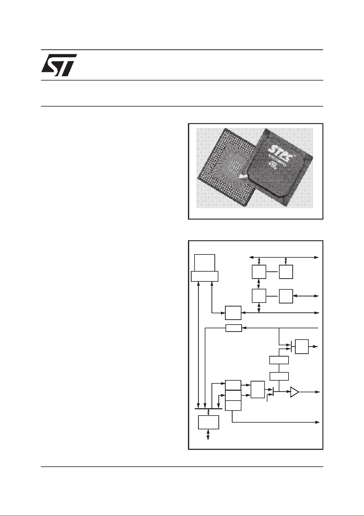
The STPC Consumer is packaged in a 388 Plastic
Ball Grid Array (PBGA).
STPC CONSUMER
PBGA388
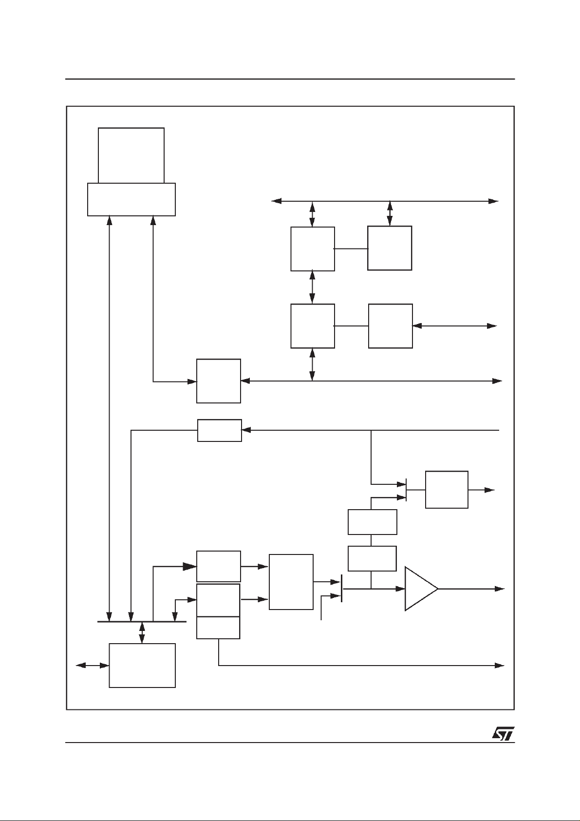
Figure 1. Logic Diagram
x86
Core
Host I/F
PCI
m/s
VIP
Video
DRAM
CTRL
pipeline
2D
SVGA
CRTC
Chroma
ISA
m/s
PCI
m/s
Color
Key
Key
HW Cursor
IPC
EIDE
AntiFlicker
Color Space
Converter
ISABUS
EIDE
PCIBUS
CCIRInput
TVOutput
Digital
PAL/
NTSC
Monitor
SYNCOutput
Issue 1.2
1/518/2/00

STPC CONSUMER
■ X86 Processor core
■ Fully static 32-bit 5-stage pipeline, x86
processor fully PC compatible.
■ Can access up to 4GBytes of external
memory.
■ 8KByte unified instruction and data cache
with write back and write through capability.
■ Parallelprocessingintegral floating pointunit,
with automatic power down.
■ Clock core speeds up to of 100 MHz.
■ Fully static design for dynamic clock control.
■ Low power and system management modes.
■ Optimized design for3.3V operation.
■ DRAM Controller
■ Integrated systemmemory andgraphic frame
memory.
■ Supports up to 128 MBytes system memory
in 4 banks and down to as little as 2Mbytes.
■ Supports 4MB, 8MB, 16MB, 32MB single-
sided and double-sided DRAM SIMMs.
■ Four quad-word write buffers for CPU to
DRAM and PCI to DRAM cycles.
■ Four 4-word read buffers for PCI masters.
■ Supports Fast Page Mode & EDO DRAM.
■ Programmable timing for DRAM parameters
including CAS pulse width, CAS pre-charge
time and RAS to CAS delay.
■ 60, 70, 80 & 100ns DRAM speeds.
■ Memory hole between 1 MByte & 8 MByte
supported for PCI/ISA busses.
■ Hidden refresh.
To check if your memory device is supported by
the STPC, please refer to Table 9-3 in the
Programming Manual.
■ Graphics Engine
■ 64-bit windows accelerator.
■ Backward compatibility to SVGA standards.
■ Hardware acceleration for text, bitblts,
transparent bltsand fills.
■ Up to 64 x 64 bit graphics hardware cursor.
■ Up to 4MB long linear frame buffer.
■ 8-, 16-, and 24-bit pixels.
■ Drivers for Windows and other operating
systems.
■ VGA Controller
■ Integrated 135MHz triple RAMDACallowing
for 1280 x 1024 x 75Hz display.
■ Requires external frequency synthesizer and
reference sources.
■ 8-, 16-, 24-bit pixels.
■ Interlaced or non-interlaced output.
■ Video Input port
■ Accepts video inputs in CCIR 601/656 or
ITU-R 601/656, and stream decoding.
■ Optional 2:1 decimator
■ Stores captured video in off setting area of
the onboard frame buffer.
■ Video pass through to the onboard PAL/
NTSC encoder forfull screen video images.
■ HSYNC and B/T generation or lock onto
external video timing source.
■ Video Pipeline
■ Two-tapinterpolative horizontal filter.
■ Two-tapinterpolative vertical filter.
■ Color space conversion (RGB to YUV and
YUV to RGB).
■ Programmable window size.
■ Chroma and color keying for integrated video
overlay.
■ Programmable two tap filter with gamma
correction or three tap flicker filter.
■ Progressiveto interlaced scan converter.
■ Digital NTSC/PAL encoder
■ NTSC-M, PAL-M,PAL-B,D,G,H,I,PAL-N easy
programmable video outputs.
■ CCIR601 encoding with programmable color
subcarrier frequencies.
■ Line skip/insert capability
■ Interlaced or non-interlaced operation mode.
■ 625 lines/50Hz or 525 lines/60Hz 8 bit
multiplexedCB-Y-CR digital input.
■ CVBS and R,G,B simultaneous analog
outputs through 10-bit DACs.
■ Cross colorreduction by specific trap filtering
on luma within CVBS flow.
■ Power down mode available on each DAC.
2/51
Issue 1.2

STPC CONSUMER
■ PCI Controller
■ Fully compliant with PCI 2.1 specification.
■ Integrated PCI arbitration interface. Up to 3
masters can connect directly. External PAL
allows for greater than 3 masters.
■ Translation of PCI cycles to ISA bus.
■ Translation of ISA master initiated cycle to
PCI.
■ Support forburst read/write from PCI master.
■
0.33X and 0.5X CPU clock PCI clock.
■ ISA master/slave Interface
■ Generates the ISA clock from either
14.318MHz oscillator clock or PCI clock
■ Supports programmable extra wait state for
ISA cycles
■ Supports I/O recovery time for back to back
I/O cycles.
■ Fast Gate A20 and Fast reset.
■
Supports the single ROM that C, D, or E.
blocks shares withF block BIOS ROM.
■ Supports flash ROM.
■ Supports ISA hidden refresh.
■ Buffered DMA &ISA master cycles to reduce
bandwidth utilizationof the PCI andHost bus.
NSP compliant.
■ IDE Interface
■ Supports PIO
■
Supports up to Mode 5 Timings
■ TransferRates to 22 MBytes/sec
■ Supports up to 4 IDE devices
■ Concurrent channel operation(PIO modes) -
4 x 32-Bit Buffer FIFOs per channel
■ Support for PIO mode 3 & 4.
■ Support for 11.1/16.6 MB/s, I/O Channel
Ready PIO data transfers.
■ Individual drive timing for all four IDE devices
■ Supports both legacy & native IDE modes
■ Supports hard drives larger than 528MB
■ Support for CD-ROM and tape peripherals
■ Backward compatibility with IDE (ATA-1).
■ Drivers for Windows and other Operating
Systems
■ Integrated peripheral controller
■ 2X8237/AT compatible 7-channel DMA
controller.
■ 2X8259/AT compatible interrupt Controller.
16 interrupt inputs - ISA and PCI.
■ Three 8254 compatible Timer/Counters.
■ Co-processor error support logic.
■ Power Management
■ Four power saving modes: On, Doze,
Standby, Suspend.
■ Programmable system activity detector
■ Supports SMM and APM.
■ Supports STOPCLK.
■ Supports IO trap & restart.
■ Independent peripheral time-out timer to
monitor hard disk, serial & parallel ports.
■ Supports RTC,interrupts and DMAs wake-up
Issue 1.2
3/51

STPC CONSUMER
4/51
Issue 1.2

UPDATE HISTORY FOR OVERVIEW.
0.1 UPDATE HISTORY FOR OVERVIEW.
The following changes have been made to the Electrical Specification Chapter on the 02/02/2000.
Section Change Text
Added
To check if your memory device is supported by the STPC, please refer to
Table 9-3 Host Address to MA Bus Mappingin the Programming Manual.
Issue 1.2
5/51

GENERAL DESCRIPTION
1. GENERAL DESCRIPTION
At the heart of the STPC Consumer is an advanced processor block, dubbed the 5ST86. The
5ST86 includes a powerful x86 processor core
along with a 64-bit DRAM controller, advanced
64bit accelerated graphics and video controller, a
high speed PCI local-bus controller and Industry
standard PC chip set functions (Interrupt controller, DMA Controller, Interval timer and ISA bus)
and EIDE controller.
The STPC Consumer has in addition to the
5ST86, a Video subsystem and high quality digital
Television output.
The STMicroelectronics x86 processorcore is embedded with standard and application specific peripheral modules on the same silicon die. The core
has all the functionality of the STMicroelectronics
standard x86 processor products, including the
low power System Management Mode (SMM).
System Management Mode (SMM) provides an
additional interrupt and address space that can be
used for system power management or software
transparent emulation of peripherals. While running in isolated SMM address space, the SMM interrupt routine can execute without interfering with
the operating system or application programs.
Further power management facilities include a
suspend mode that can be initiated from either
hardware or software.Because of the static nature
of the core, no internal data is lost.
The STPC Consumer makes use of a tightly coupled Unified Memory Architecture (UMA), where
the same memory array is used for CPU main
memory and graphics frame-buffer. This significantly reduces total system memory with system
performances equal to that of a comparable solution with separate frame buffer and system memory. In addition, memory bandwidth is improved by
attaching the graphics engine directly to the 64-bit
processor host interface running at the speed of
the processor bus rather than the traditional PCI
bus.
The 64-bit wide memory array provides the system with 320MB/s peak bandwidth, double that of
an equivalent system using 32 bits. This allows for
higher screen resolutions and greater color depth.
The processor bus runs at the speed of the processor (DX devices) or half the speed (DX2 devices).
The ‘standard’ PC chipset functions (DMA, interrupt controller, timers, power management logic)
are integrated with the x86 processor core.
The PCI bus is the main data communication link
to the STPC Consumer chip. The STPC Consumer translates appropriate host bus I/O and Memory
cycles onto the PCI bus. It also supports the generation of Configuration cycles on the PCI bus.
The STPC Consumer, as a PCI bus agent (host
bridge class), fully complies with PCI specification
2.1. The chip-set also implements the PCI mandatory header registers in Type 0 PCI configuration
space for easy porting of PCI aware system BIOS. The device contains a PCI arbitration function
for three external PCI devices.
The STPC Consumer integrates an ISA bus controller. Peripheral modules such as parallel and
serial communications ports, keyboard controllers
and additional ISA devices can be accessed by
the STPC Consumer chip set through this bus.
An industry standard EIDE (ATA 2) controller is
built in to the STPC Consumer and connected internally via the PCI bus.
Graphics functions are controlled by the on-chip
SVGA controller and the monitor display is managed by the 2D graphics display engine.
This Graphics Engine is tuned to work with the
host CPU to provide a balanced graphics system
with a low silicon area cost. It performs limited
graphics drawing operations, which include hardware acceleration of text, bitblts, transparent blts
and fills. These operations can act on off-screen
or on-screen areas. The frame buffer size ranges
up to 4 Mbytes anywhere in the physical main
memory.
The graphics resolution supported is a maximum
of 1280x1024 in 65536 colours at 75Hz refresh
rate and is VGA and SVGA compatible. Horizontal
timing fields are VGA compatible while the vertical
fields are extendedby one bit to accommodate the
above display resolution.
STPC Consumer providesseveral additional functions to handle MPEG or similar video streams.
The Video Input Port accepts an encoded digital
video stream in one of a number of industry standard formats, decodes it, optionally decimates it by
a factor of 2:1, and deposits it into an off screen
area of the frame buffer. An interrupt request can
be generated when an entire field or frame has
been captured.
6/51
Issue 1.2

GENERAL DESCRIPTION
The video output pipeline incorporates a videoscaler andcolor spaceconverter function and provisions in the CRT controller to display a video
window. Whilerepainting the screen the CRT controller fetchesboth the video as well as the normal
non-video frame buffer in two separate internal
FIFOs (256-Bytes each). The video stream can be
color-space converted (optionally) and smooth
scaled. Smooth interpolative scaling in both horizontal and vertical directions are implemented.
Color and Chroma key functions are also implemented to allow mixing video stream with non-video frame buffer.
The video output passes directly to the RAMDAC
for monitor output or through another optional
color spaceconverter (RGB to 4:2:2 YCrCb) to the
programmable anti-flicker filter. The flicker filter is
configured as either a two line filter with gamma
correction (primarily designed for DOS type text)
or a 3 line flicker filter (primarily designed for Windows type displays). The flicker filter is optional
and can be softwaredisabled foruse with video on
large screen areas.
The Video output pipeline of the STPC Consumer
interfaces directly to the internal digital TV encoder. It takes a 24 bit RGB non-interlaced pixel
stream and converts to a multiplexed 4:2:2 YCrCb
8 bit output stream, the logic includes a progressive to interlaced scan converter and logic to insert appropriate CCIR656 timing reference codes
into the output stream. It facilitates the high quality
display of VGA or full screen video streams received via the Video input port to standard NTSC
or PAL televisions.
The STPC Consumer core is compliant with the
Advanced Power Management (APM) specification to provide a standard method by which the
BIOS can control the power used by personal
computers. The Power Management Unit module
(PMU) controls the power consumption by providing a comprehensive set of features that control
the power usage and supports compliance with
the United States EnvironmentalProtection Agency’s Energy Star Computer Program. The PMU
provides following hardware structures to assist
the software in managing the power consumption
by the system.
- System Activity Detection.
- 3 power-down timers detecting system inactivity:
- Doze timer (short durations).
- Stand-by timer (medium durations).
- Suspend timer (long durations).
- House-keeping timer to cope with short bursts of
house-keeping activity while dozing or in stand-by
state.
- Peripheral activity detection.
- Peripheral timer detecting peripheral inactivity
- SUSP# modulationto adjust the system performance in various power down states of the system
including full power on state.
- Power control outputs to disable power from different planes of the board.
Lack of system activity for progressively longer
period of times is detected by the three power
down timers. These timers can generate SMI interrupts to CPU so that the SMM software can put
the system in decreasing states of power consumption. Alternatively, system activity in a power
down statecan generate SMI interrupt to allow the
software to bring the system back up to full power
on state. The chip-set supports up to three power
down states: Doze state, Stand-by state and Suspend mode. These correspond to decreasing levels of power savings.
Power down puts the STPC Consumer into suspend mode. The processor completes execution
of thecurrent instruction, any pending decoded instructions and associated bus cycles. During the
suspend mode, internal clocks are stopped. Removing power down, the processor resumes instruction fetching and begins execution in the instruction stream at the point it had stopped.
A reference design for the STPC Consumer is
available including the schematics and layout
files, the design is a PC ATX motherboard design.
The design is available as a demonstration board
for application and systemdevelopment.
The STPC Consumer is supported by several
BIOS vendors, including the super I/O device
used in the reference design. Drivers for 2D accelerator, video features and EIDE are availaible on
various operating systems.
The STPC Consumer has been designed using
modern reusable modular design techniques, it is
possible to add orremove the standard features of
the STPC Consumer or other variants of the
5ST86 family. Contact your local STMicroelectonics sales office for further information.
- House-keeping activity detection.
7/51
Issue 1.2
GENERAL DESCRIPTION
Figure 1-1 Functionnal description
x86
Core
Host I/F
ISA BUS
PCI m/s
VIP
ISA
PCI m/s
IPC
EIDE
Anti-Flicker
EIDE
PCI BUS
CCIR Input
TV Output
Digital
PAL/
8/51
DRAM
Video
pipeline
2D
SVGA
CRTC
Color
Key
Chroma
Issue 1.2
Color Space
Monitor
HW Cursor
SYNC Output

Figure 1-2 Typical Application
Super I/O
GENERAL DESCRIPTION
Keyboard / Mouse
Serial Ports
Parallel Port
ISA
MUX
MUX
DMUX
RTC
Flash
IRQ
DMA.REQ
STPC Consumer
DMA.ACK
Floppy
2x EIDE
DMUX
Monitor
SVGA
TV
S-VHS
RGB
PAL
NTSC
PCI
Video
CCIR601
CCIR656
4x 16-bit EDO DRAMs
9/51
Issue 1.2
PIN DESCRIPTION
2. PIN DESCRIPTION
2.1 INTRODUCTION
The STPC Consumer integrates most of the functionalities of the PC architecture. As a result, many
of the traditional interconnections between the
host PC microprocessor and the peripheral devices aretotally internal to the STPC Consumer.This
offers improved performance due to the tight coupling of the processor core and these peripherals.
As a result many of the external pin connections
are made directly to the on-chip peripheral functions.
Figure 2-1 shows the STPC Consumer’s external
interfaces. It defines the main busses and their
function. Table 2-1 describes the physical implementation listing signal types and their functionalities. Table 2-2 provides a full pin listing and description. Table 2-3 provides a full listing of the
STPC Consumer pin locations of package by
physical connection. Please refer to the pin allocation drawing for reference.
Figure 2-1. STPC Consumer External Interfaces
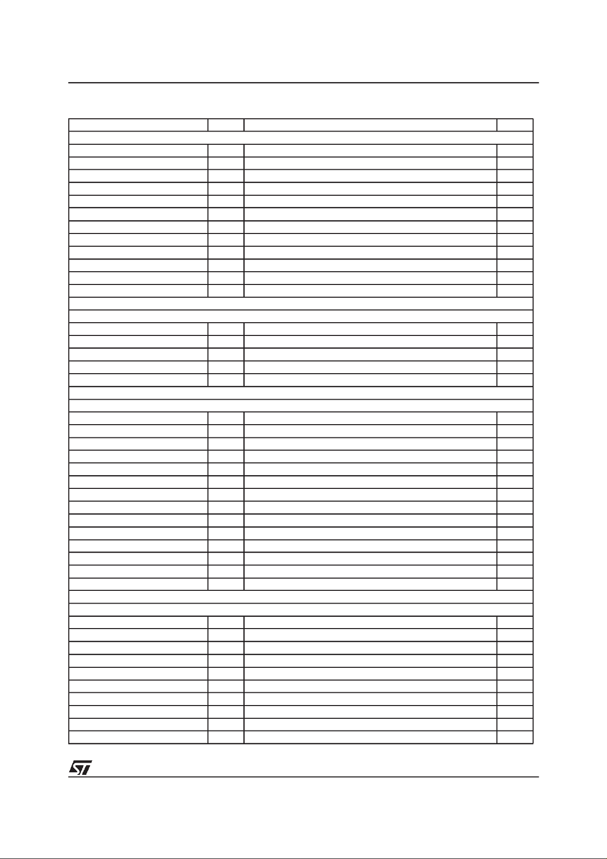
Table 2-1. Signal Description
Group name Qty
Basic Clocks reset & Xtal(SYS) 12
DRAM Controller 89
PCI interface (PCI) 58
ISA / IDE / IPC combined interface 88
Video Input (VIP) 9
TV Output 10
VGA Monitor interface 10
Grounds 69
V
DD
Analog specific V
Reserved 5
Total Pin Count 388
CC/VDD
26
12
Note: Several interface pins are multiplexed with
other functions, refer to the Pin Description section for further details
x86
STPC Consumer
SOUTHNORTH PCI
DRAM VGA VIP TV SYS ISA/IDE IPC
89 10 9 10 58
10/51
Issue 1.2
13
77 11
PIN DESCRIPTION
Table 2-2. Definition of Signal Pins
Signal Name Dir Description Qty
BASIC CLOCKS AND RESETS
SYSRSTI# I System Reset / Power good 1
XTALI I 14.3MHz Crystal Input 1
XTALO I/O 14.3MHz Crystal Output - External Oscillator Input 1
HCLK O Host Clock (Test) 1
DEV_CLK O 24MHz Peripheral Clock (floppy drive) 1
GCLK2X I/O 80MHz Graphics Clock 1
DCLK I/O 135MHz Dot Clock 1
PCI_CLKI I 33MHz PCI Input Clock 1
PCI_CLKO O 33MHz PCI Output Clock (from internal PLL) 1
SYSRSTO# O Reset Output to System 1
ISA_CLK O ISA Clock Output - Multiplexer Select Line For IPC 1
ISA_CLK2X O ISA Clock x 2 Output - Multiplexer Select Line For IPC 1
MEMORY INTERFACE
MA[11:0] I/O Memory Address 12
RAS#[3:0] O Row Address Strobe 4
CAS#[7:0] O Column Address Strobe 8
MWE# O Write Enable 1
MD[63:0] I/O Memory Data 64
PCI INTERFACE
AD[31:0] I/O PCI Address / Data 32
CBE[3:0] I/O Bus Commands / Byte Enables 4
FRAME# I/O Cycle Frame 1
TRDY# I/O Target Ready 1
IRDY# I/O Initiator Ready 1
STOP# I/O Stop Transaction 1
DEVSEL# I/O Device Select 1
PAR I/O Parity Signal Transactions 1
SERR# O System Error 1
LOCK# I PCI Lock 1
PCIREQ#[2:0] I PCI Request 3
PCIGNT#[2:0] O PCI Grant 3
PCI_INT[3:0] I PCI Interrupt Request 4
VDD5 I 5V Power Supply for PCI ESD protection 4
ISA AND IDE COMBINED ADDRESS/DATA
LA[23:22] / SCS3#,SCS1# I/O Unlatched Address (ISA) / Secondary Chip Select (IDE) 2
LA[21:20] / PCS3#,PCS1# I/O Unlatched Address (ISA) / Primary Chip Select (IDE) 2
LA[19:17] / DA[2:0] O Unlatched Address (ISA) / Address (IDE) 3
RMRTCCS# / DD[15] I/O ROM/RTC Chip Select / Data Bus bit 15 (IDE) 1
KBCS# / DD[14] I/O Keyboard Chip Select / Data Bus bit 14 (IDE) 1
RTCRW# / DD[13] I/O RTC Read/Write / Data Bus bit 13 (IDE) 1
RTCDS# / DD[12] I/O RTC Data Strobe / Data Bus bit 12 (IDE) 1
SA[19:8] / DD[11:0] I/O Latched Address (ISA) / Data Bus (IDE) 16
SA[7:0] I/O Latched Address (IDE) 4
SD[15:0] I/O Data Bus (ISA) 16
Issue 1.2
11/51
PIN DESCRIPTION
Table 2-2. Definition of Signal Pi ns
Signa l Name Dir Description Qty
ISA/IDE COMBINED CONTROL
IOCHRDY / DIORDY I/O I/O Channel Ready (ISA) - Busy/Ready (IDE) 1
ISA CONTROL
OSC14M O ISA bus synchronisation clock 1
ALE O Address Latch Enable 1
BHE# I/O System Bus High Enable 1
MEMR#, MEMW# I/O Memory Read and Memory Write 2
SMEMR#, SMEMW# O System Memory Read and Memory Write 2
IOR#, IOW# I/O I/O Read and Write 2
MASTER# I Add On Card Owns Bus 1
MCS16#, IOCS16# I Memory/IO Chip Select16 2
REF# O Refresh Cycle. 1
AEN O Address Enable 1
ZWS# I Zero Wait State 1
IOCHCK# I I/O Channel Check. 1
ISAOE# O Bidirectional OE Control 1
RTCAS# O Real Time Clock Address Strobe 1
GPIOCS# I/O General Purpose Chip Select 1
IDE CONTROL
PIRQ I Primary Interrupt Request 1
SIRQ I Secondary Interrupt Request 1
PDRQ I Primary DMA Request 1
SDRQ I Secondary DMA Request 1
PDACK# O Primary DMA Acknowledge 1
SDACK# O Secondary DMA Acknowledge 1
PIOR# I/O Primary I/O Read 1
PIOW# O Primary I/O Write 1
SIOR# I/O Secondary I/O Read 1
SIOW# O Secondary I/O Write 1
IPC
IRQ_MUX[3:0] I Multiplexed Interrupt Request 4
DREQ_MUX[1:0] I Multiplexed DMA Request 2
DACK_ENC[2:0] O DMA Acknowledge 3
TC O ISA Terminal Count 1
MONITOR INTERFACE
RED, GREEN, BLUE O Red, Green, Blue 3
VSYNC O Vertical Sync 1
HSYNC O Horizontal Sync 1
VREF_DAC I DAC Voltage reference 1
RSET I Resistor Set 1
COMP I Compensation 1
DDC[1:0] I/O Display Data Channel Serial Link 2
SCL / DDC[1] I/O I C Inte rface - Clock / Can be used for VGA DDC[1] signal 1
12/51
Issue 1.2
PIN DESCRIPTION
Table 2-2. Definition of Signal Pi ns
Signa l Name Dir Description Qty
SDA / D DC[0] I/O I C Inte rface - Data / Can be used for VGA D DC[0] signal 1
COL_CMP O Color Compare Output.
VIDEO INPUT
VCLK I Pixel Clock 1
VIN I YUV Video D ata I nput CCIR 601 or 656 8
DIGITAL TV O UTPUT
RED_TV, GR EEN_TV, BLUE_TV O Analog video outputs s ynchronized with CVBS 3
VCS O Composite Synch or Ho rizontal line SYN C output 1
ODD_EVEN O Frame Synchronisation 1
CVBS O Analog video com posite output (luminance / chrom inance) 1
IREF1_ TV I Reference cu rrent of 9bit DA C for CVBS 1
VREF1_TV I Reference vo ltage of 9b it DA C for CV BS 1
IREF2_ TV I Reference cu rrent of 8bit DA C for R,G,B 1
VREF2_TV I Reference vo ltage of 8b it DA C for R,G ,B 1
VSSA_T V I Analog Vss f or DAC 1
VDDA_TV I Analog Vdd for DAC 1
MISCEL LANE OUS
SPKRD O Speaker Dev ice O utput 1
SCAN_ENAB LE I Reserved (Test pin) 1
Issue 1.2
13/51

PIN DESCRIPTION
2.2 SIGNAL DESCRIPTIONS
2.2.1 BASIC CLOCKS AND RESETS
SYSRSTI
System Reset/Power good.
This input is
low when the reset switch is depressed. Otherwise, it reflects the power supply’s power good
signal. SYSRSTI is asynchronous to all clocks,
and acts as a negative active reset. The reset circuit initiates a hard reset on the rising edge of
SYSRSTI.
SYSRSTO#
Reset Output to System.
This is the
system resetsignal and is used to reset the rest of
the components (not on Host bus) in the system.
The ISA bus reset is an externally inverted buffered versionof this output and the PCI bus reset is
an externally buffered version of this output.
XTALI
XTALO
14.3MHz Crystal Input
14.3MHz Crystal Output.
These pins are
the 14.318MHz crystalinput; This clock isused as
the reference clock for the internal frequency synthesizer to generate the HCLK, CLK24M,
GCLK2X and DCLK clocks.
A 14.318 MHz Series Cut Quartz Crystal should
be connected between these two pins. Balance
capacitors of 15 pF should also be added. In the
event of an external oscillatorproviding the master
clock signal to the STPC Consumer device, the
TTL signal should be provided on XTALO.
HCLK
Host Clock.
This is the host 1X clock. Its
frequency can vary from 25 to 75 MHz. All host
transactions and PCI transactions are synchronized to this clock. The DRAM controller to execute the host transactions is also driven by this
clock. In normal mode, this output clock is generated by the internal pll.
GCLK2X
80MHz Graphics Clock.
This is the
Graphics 2X clock, which drives the graphics engine and the DRAM controller to execute the
graphics and display cycles.
Normally GCLK2Xis generated by the internal frequency synthesizer, and this pin is an output. By
setting a bit in Strap Register 2, this pin can be
made an input so that an external clock can replace the internal frequency synthesizer.
DCLK
135MHz Dot Clock.
This is the dot clock,
which drivesgraphics display cycles.Its frequency
can go from 8MHz (using internal PLL) up to 135
MHz, and it is required to have a worst case duty
cycle of 60-40.
This signal iseither driven by the internal pll (VGA)
or an external 27MHz oscillator (when the composite video output is enabled). The direction can
be controlled by a strap option or an internal register bit.
ISA_CLK
lect Line For IPC).
ISA Clock Output (also Multiplexer Se-
This pin produces the Clock
signal for the ISA bus. It is also used with
ISA_CLK2X as the multiplexorcontrol lines for the
Interrupt Controller Interrupt input lines. This is a
divided down version of either the PCICLK or
OSC14M.
ISA_CLKX2
Select Line For IPC).
ISA Clock Output (also Multiplexer
This pin produces a signal
that is twice the frequency of the ISA bus Clock
signal. It is also used with ISA_CLK as the multiplexor control lines for the Interrupt Controller input lines.
DEV_CLK
24MHz Peripheral Clock Output.
This
24MHZ signal is provided as a convenience for
the system integration of a Floppy Disk driver
function in an external chip.
OSC14M
ISA bus synchronisation clock Output.
This is the buffered 14.318 Mhz clock to the ISA
bus.
2.2.2 MEMORY INTERFACE
MA[11:0]
Memory Address Output.
These 12 multiplexed memory address pins support external
DRAM with up to 4K refresh. These include all
16M x N and some 4M x N DRAM modules. The
address signals must be externally buffered to
support more than 16 DRAM chips. The timing of
these signals can be adjusted by software to
match the timings of most DRAM modules.
PCI_CLKI
33MHz PCI Input Clock
This signal is the PCI bus clock input and should
be driven from the PCI_CLKO pin.
PCI_CLKO
33MHz PCI Output Clock.
This is the
master PCI bus clock output.
14/51
Issue 1.2

PIN DESCRIPTION
MD[63:0]
Memory Data I/O.
This is the 64-bit
memory data bus. If only half of a bank is populated, MD63-32 is pulled high, data is on MD31-0.
MD[40-0] are read by the device strap option registers during rising edge of SYSRSTI.
RAS#[3:0]
Row Address Strobe Output.
There
are 4 active low row address strobe outputs, one
for each bank of the memory. Each bank contains
4 or 8-Bytes of data. The memory controllerallows
half of a bank (4-bytes) to be populated to enable
memory upgrade at finer granularity.
The RAS# signals drive the SIMMs directly without any external buffering. These pins are always
outputs, but they can also simultaneously be inputs, toallow the memory controller to monitor the
value of the RAS# signals at the pins.
CAS#[7:0]
Column Address Strobe Output.
There
are 8 active low column address strobe outputs,
one each for each byte of the memory.
The CAS# signals drive the SIMMs either directly
or through external buffers.
These pins are always outputs, but they can also
simultaneously be inputs, to allow the memory
controller to monitor the value of the CAS# signals
at the pins.
MWE#
Write Enable Output.
Write enable specifies whether the memory access is a read (MWE#
= H) or a write (MWE# = L). This single write enable controls all the DRAM. It can be externally
buffered to boost the maximum number of loads
(DRAM chips) supported.
The MWE# signals drive the SIMMs directly without any external buffering.
simple analog low pass filter is recommended. In
S-VHS mode, this is the Chrominance Output.
GREEN_TV / Y_TV
chronized with CVBS.
Analog video outputs syn-
This output is current-driven and must be connected to analog ground over
a load resistor (R
). Following the load resis-
LOAD
tor, a simple analog low pass filter is recommended. In S-VHS mode, this is the Luminance Output.
BLUE_TV / CVBS
nized withCVBS.
Analog video outputs synchro-
This outputis current-driven and
must be connected to analog ground over a load
resistor (R
simple analog low pass filter is recommended. In
). Following the load resistor, a
LOAD
S-VHS mode, this is a second composite output.
VCS
Line synchronisation Output.
This pin is an
input in ODDEV+HSYNC or VSYNC + HSYNC or
VSYNC slave modes and an output in all other
modes (master/slave)
The signal is synchronous to rising edge of CKREF. The default polarity uses a negative pulse
ODD_EVEN
Frame Synchronisation Ourput.
This
pin supports the Frame synchronisation signal. It
is an input in slave modes, except when sync is
extracted from YCrCb data, and an output in master mode and when sync is extracted from YCrCb
data
The signal is synchronous to rising edge of DCLK.
The default polarity for this pin is:
- odd (not-top) field : LOW level
- even (bottom) field : HIGH level
IREF1_TV
Ref. current
for CVBS 10-bit DAC.
2.2.3 VIDEO INTERFACE
VCLK
VIN[7:0]
Pixel Clock Input.
YUV Video Data Input CCIR 601 or 656.
Time multiplexed 4:2:2 luminance and chrominance data as defined in ITU-R Rec601-2 and
Rec656 (except for TTL input levels). This bus interfaces with an MPEG video decoder output port
and typically carries a stream of Cb,Y,Cr,Y digital
video at VCLK frequency, clocked on the rising
edge (by default) of VCLK. A 54-Mbit/s ‘double’
Cb, Y, Cr, Y inputmultiplex is supported for double
encoding application (rising and falling edge of
CKREF are operating).
2.2.4 TV OUTPUT
RED_TV / C_TV
nized with CVBS.
Analog video outputs synchro-
This outputis current-driven and
must be connected to analog ground over a load
resistor (R
). Following the load resistor, a
LOAD
VREF1_TV
IREF2_TV
VREF2_TV
VSSA_TV
VDDA_TV
CVBS
chrominance).
Ref. voltage
Reference current
Reference voltage
for CVBS 10-bit DAC.
for RGB 9-bit DAC.
forRGB 9-bit DAC.
Analog VSSfor DAC
Analog VDDfor DAC
Analog video composite output (luminance/
CVBS is current-driven and must
be connected to analog ground over a load resistor (R
). Following the load resistor, a simple
LOAD
analog low pass filter is recommended.
2.2.5 PCI INTERFACE
AD[31:0]
PCI Address/Data.
This is the 32-bit
multiplexed address and data bus of the PCI. This
bus is driven by the master during the address
phase and data phase of write transactions. It is
Issue 1.2
15/51

PIN DESCRIPTION
driven by the target during data phase of read
transactions.
CBE#[3:0]
Bus Commands/Byte Enables.
These
are the multiplexed command and byte enable
signals of the PCI bus. During the address phase
they define the command and during the data
phase they carry the byte enable information.
These pins are inputs when a PCI master other
than the STPC Consumer owns the bus and outputs when the STPC Consumer owns the bus.
FRAME#
Cycle Frame.
This is the frame signal of
the PCIbus. Itis an input when a PCI master owns
the bus and is an output when STPC Consumer
owns the PCI bus.
TRDY#
Target Ready.
This is the target ready signal of the PCI bus. It is driven as an output when
the STPC Consumer is the target of the current
bus transaction. It is used as an input when STPC
Consumer initiates a cycle on the PCI bus.
IRDY#
Initiator Ready.
This is the initiator ready
signal of the PCI bus. It is used as an output when
the STPC Consumer initiates a bus cycle on the
PCI bus. It is used as an input during the PCI cycles targeted to the STPC Consumer to determine
when the current PCI master is ready to complete
the current transaction.
STOP#
Stop Transaction.
Stop is used to implement the disconnect, retry and abort protocol of
the PCI bus. It is used as an input for the bus cycles initiated by the STPC Consumer and is used
as an output when a PCI master cycle is targeted
to the STPC Consumer.
DEVSEL#
I/O Device Select.
This signal is used
as an input when the STPC Consumer initiates a
bus cycle on the PCI bus to determine if a PCI
slave device has decoded itself to be the target of
the current transaction. It is asserted as an output
either when the STPC Consumer is the target of
the current PCI transaction or when no other device asserts DEVSEL# prior to the subtractive decode phase of the current PCI transaction.
SERR#
System Error.
This is the system error signal of the PCI bus. It may, if enabled, be asserted
for one PCI clock cycle if target aborts a STPC
Consumer initiated PCI transaction. Its assertion
by either the STPC Consumer or by another PCI
bus agent will trigger the assertion of NMI to the
host CPU. This is an open drain output.
LOCK#
PCI Lock.
This is the lock signal of the PCI
bus and is used to implement the exclusive bus
operations when acting as a PCI target agent.
PCIREQ#[2:0]
PCI Request.
This pin are the
three external PCI master request pins. They indicates to the PCI arbiter that the external agents
desire use of the bus.
PCIGNT#[2:0]
PCI Grant.
These pins indicate that
the PCI bus has been granted to the master requesting it on its PCIREQ#.
2.2.6 ISA/IDE COMBINED ADDRESS/DATA
LA[23]/SCS3#
ary Chip Select (IDE).
Unlatched Address (ISA)/Second-
This pin has two functions,
depending on whether the ISA bus is active or the
IDE bus is active.
When the ISA bus is active, this pins is ISA Bus
unlatched address bit 23 for 16-bit devices. When
ISA bus is accessed by any cycle initiated from
PCI bus, this pin is in output mode. When an ISA
bus master owns the bus, this pins is in input
mode.
When the IDE bus is active, this signals is used as
the active high secondary slave IDE chip select
signal. This signal is to be externally NANDed with
the ISAOE# signal before driving the IDE devices
to guarantee it is active only when ISA bus is idle.
PAR
Parity Signal Transactions.
This is the parity
signal of the PCI bus. This signal is used to guarantee even parity across AD[31:0], CBE#[3:0],
and PAR. This signal is driven by the master during the address phase and data phase of write
transactions. It is driven by the target during data
phase of read transactions. (Its assertion is identical to that of theAD bus delayed by one PCIclock
cycle)
16/51
Issue 1.2
 Loading...