

SGS Thomson Microelectronics STPAC01F1 Datasheet
®
IPAD
TM
MAIN PRODUCT CHARACTERISTICS
The STPAC01F1 has two outputs, one for the
signal detection and another one for the
temperature compensation:
V
■
■
■
= 0.88 V at 0.85 GHz at 10 dBm
DCout
V
= 1.07 V at 1.85 GHz at 10 dBm
DCout
Vsupply=5Vmax.
DESCRIPTION
The STPAC01isanintegrated RF detector for the
power control stage. It converts RF signal coming
from the coupler into a DC signal usable by the
digital stage. It is based on the use of two similar
diodes, one providing the signal detection while
the second one is used to provide a temperature
information to thermal compensation stage. A
biasing stage suppresses the detection diode drop
voltage effect.
Target applications are cellular phones and PDA
using GSM, DCS, PCS, AMPS, TDMA , CDMA
and 800MHz to 1900MHz frequency ranges
STPAC01F1
RF DETECTOR FOR
POWER AMPLIFIER CONTROL
Flip-Chip package
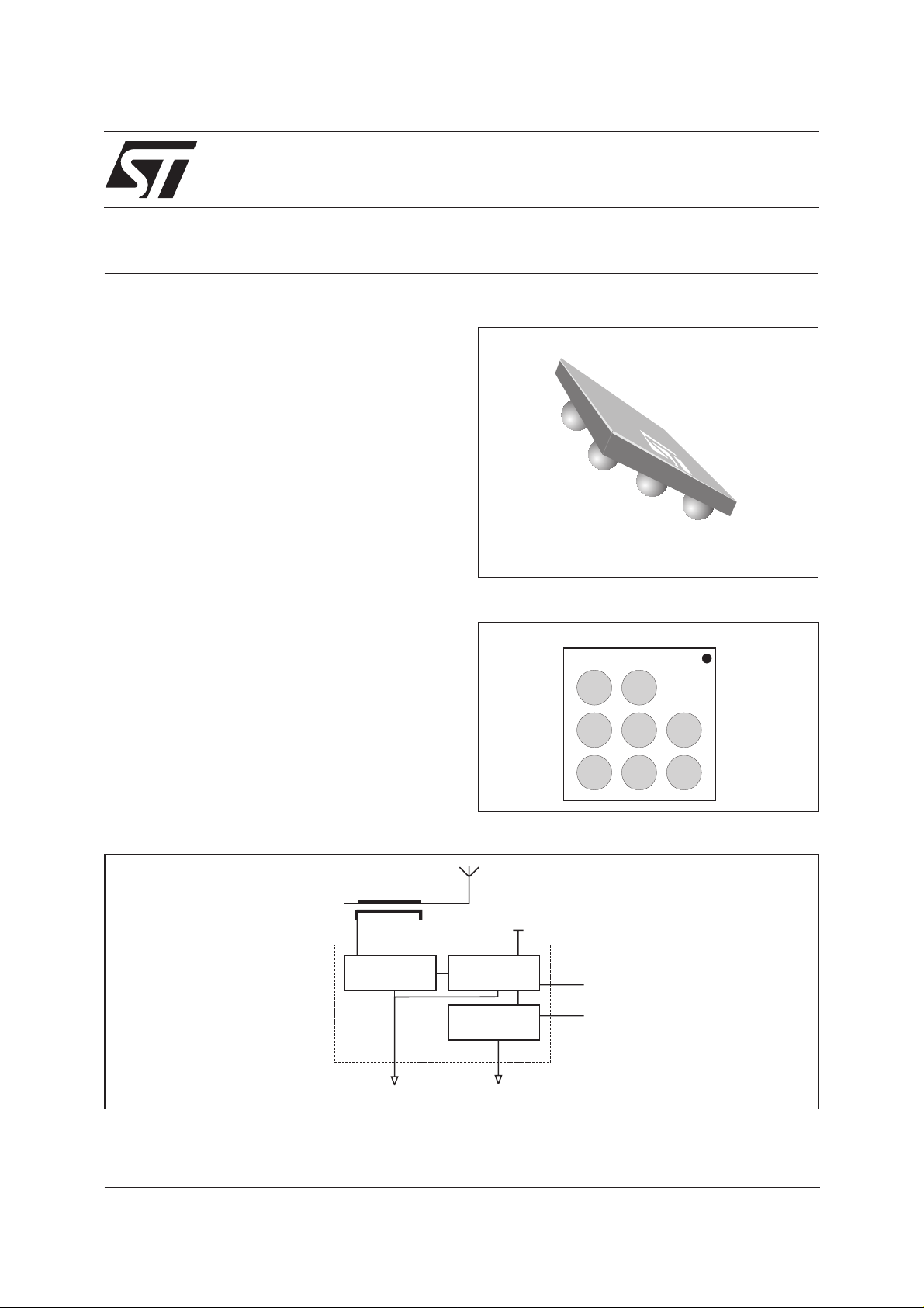
PIN CONFIGURATION (ball side)
321
DC
out
V
Temp
A
BENEFITS
■
The use of IPAD technology allows the RF
front-end designer to save PCB area and to
drastically suppress parasitic inductances.
FUNCTIONAL DIAGRAM
Coupler
RF input
RF detector
TM : IPAD is a trademark of STMicroelectronics.
January 2003 - Ed: 1
compensation
STPAC01F1
V
Low pass
filter
Thermal
GND2GND1
BIAS
V
V
DCOut
temp
Gnd1
RFin
Gnd1
Gnd1
Gnd2
Bias
B
C
1/6

STPAC01F1
ABSOLUTE RATINGS (Tamb = 25°C)
Symbol Parameter and test conditions Value Unit
V
BIAS
P
RF
F
OP
V
PP
T
OP
T
STG
ELECTRICAL CHARACTERISTICS (Tamb = 25°C)
PARAMETERS RELATED TO BIAS VOLTAGE
Symbol Parameter Test conditions Min. Typ. Max. Unit
V
BIAS
I
BIAS
Bias voltage
RF power at the RF input
Operating frequency range
ESD level as per MIL-STD 883E method 3015.7 notice 8 (HBM)
Operating temperature range
Storage temperature range
Operating bias voltage
Bias current V
BIAS
= 3.2 V
2.2 3.2 V
5V
20 dBm
0.8 to 2 GHz
100 V
-30 to +85 °C
-55 to 150 °C
0.5 mA
PARAMETERS RELATED TO DETECTION FUNCTION (V
= 2.7 V, DC output load = 100 kΩ)
BIAS
Symbol Parameter Test conditions Min. Typ. Max. Unit
V
∆V
DCout
DCout
DC output voltage
(see fig. 1, I
= 50µA)
DC
DCoutput voltage variation
(see fig. 5, I
= 50µA)
DC
F = 1.85 GHz, P
F = 1.85 GHz, P
F = 0.85 GHz, P
F = 0.85 GHz, P
0<T
amb
< 70°C,
F = 1.85 GHz, P
2.2<V
BIAS
< 3.2 V,
F = 1.85 GHz, P
=10dBm
RF
= -20 dBm
RF
=10dBm
RF
= -20 dBm
RF
=10dBm
RF
=10dBm
RF
0.97 1.07 1.17 V
1.83 1.93 2.03
0.78 0.88 0.98
1.83 1.93 2.03
0.09 V
0.44
PARAMETERS RELATED TO TEMPERATURE FUNCTION
Symbol Parameter Test conditions Min. Typ. Max. Unit
V
Temp
Temperature output
IDC= 50µA
1.83 1.93 2.03 V
voltage (see fig. 6)
∆V
Temp
Temperature output
voltage variation
(see fig. 6)
IDC= 50µA,0<T
= 50µA, 2.2 < V
I
DC
amb
BIAS
<70°C
< 3.2 V
0.09 V
0.44
2/6
 Loading...