

SGS Thomson Microelectronics STP9NC60FP, STP9NC60 Datasheet

STP9NC60
N - CHANNEL 600V- 0.6Ω - 9A TO-220/TO-220FP
TYPE V
ST P9 NC60
ST P9 NC60FP
ν TYPICALR
ν EXTREMELYHIGHdv/dtCAPABILITY
ν 100%AVALANCHETESTED
ν NEWHIGH VOLTAGE BENCHMARK
ν GATECHARGE MINIMIZED
DS(on)
DSS
600 V
600 V
= 0.6 Ω
DESCRIPTION
The PowerMESHII is the evolution of the first
generation of MESH OVERLAY. The layout
refinements introduced greatly improve the
Ron*area figure of merit while keeping the device
at the leading edge for what concerns switching
speed, gate charge and ruggedness.
APPLICATIONS
ν HIGHCURRENT, HIGH SPEEDSWITCHING
ν SWITHMODE POWERSUPPLIES (SMPS)
ν DC-ACCONVERTERSFOR WELDING
EQUIPMENTAND UNINTERRUPTIBLE
POWERSUPPLIESAND MOTORDRIVER
R
DS(on)
<0.75Ω
<0.75Ω
I
D
9.0 A
5.2 A
STP9NC60FP
PowerMESH ΙΙ MOSFET
3
2
1
TO-220 TO-220FP
INTERNAL SCHEMATIC DIAGRAM
3
2
1
ABSOLUTE MAXIMUM RATINGS
Symbol Parameter Value Uni t
ST P9NC6 0 ST P9 NC60FP
V
V
V
I
DM
P
dv/dt(
V
T
(•) Pulse width limited by safe operating area (1)ISD≤ 9A, di/dt ≤ 200 A/µs, VDD≤ V
February 2000
Drain-source Vol t age (VGS= 0) 600 V
DS
Drain- gate V oltage (RGS=20kΩ)
DGR
Gate-s ource Voltage ± 30 V
GS
I
Drain C urr ent (c ont inuous) at Tc=25oC9.05.2A
D
Drain C urr ent (c ont inuous) at Tc= 100oC5.73.3A
I
D
600 V
(•) Drain Curr ent (p ulsed) 36 36 A
Tot al Dissipation at Tc=25oC 125 40 W
tot
Derating Fact or 1.0 0.32 W/
1) Peak Di ode Rec ov ery v olt a ge slope 4.5 4.5 V/ ns
Insulation Withstand Voltage (DC) 2000 V
ISO
St orage Te mper ature -65 to 150
stg
T
Max. Oper ating Ju nction Tem perat ure 150
j
(BR)DSS
,Tj≤T
JMAX
o
C
o
C
o
C
1/9
STP9NC60/FP
THERMAL DATA
TO-220 TO - 220FP
R
thj-cas e
R
thj-amb
R
thc-sin k
T
AVALANCHE CHARACTERISTICS
Symb ol Parameter Max Val ue Uni t
I
AR
E
Therma l Resist ance Junction- case Max 1.0 3. 12
Therma l Resist ance Junction- ambient Max
Therma l Resist ance Case-sink Typ
Maxim um Lea d Te m pe rat ur e For Soldering Purpose
l
Avalanc h e Current, Repetit ive or Not-Repetitive
(pulse width limited by T
Single Pulse Av alanche E nergy
AS
(starting T
=25oC, ID=IAR,VDD=50V)
j
max, δ <1%)
j
62.5
0.5
300
9A
850 mJ
o
C/W
o
C/W
o
C/W
o
C
ELECTRICAL CHARACTERISTICS (T
=25oC unlessotherwisespecified)
case
OFF
Symb ol Param et er Test C o n diti o n s Mi n . Typ . Max. Unit
V
(BR) DSS
Drain-s ource
= 250 µAVGS=0
I
D
600 V
Break down Voltage
I
DSS
I
GSS
Zero G ate Voltage
Drain Current (V
GS
Gate-body Leak a ge
Current (V
DS
=0)
=0)
V
=MaxRating
DS
= Max Rating Tc= 125oC
V
DS
= ± 30 V
V
GS
1
50
± 100 nA
ON (∗)
Symb ol Param et er Test C o n diti o n s Mi n . Typ . Max. Unit
V
GS(th)
R
DS(on)
Gate Thre shold Voltage
Static Drain- s ource O n
V
DS=VGSID
=250µA
VGS= 10V ID=4A 0.6 0.75 Ω
234V
Resistance
I
D(on)
On State Drain Current VDS>I
D(on)xRDS(on)max
9.0 A
VGS=10V
DYNAMIC
Symb ol Param et er Test C o n diti o n s Mi n . Typ . Max. Unit
g
(∗)Forward
fs
Transconductance
Input Capacitance
iss
Output Capacitance
Reverse Transfer
rss
C
C
oss
C
Capacit ance
VDS>I
D(on)xRDS(on)maxID
=4A 10 S
VDS=25V f=1MHz VGS= 0 1400
196
31
µA
µA
pF
pF
pF
2/9
STP9NC60/FP
ELECTRICAL CHARACTERISTICS (continued)
SWITCHING ON
Symb ol Param et er Test C o n diti o n s Mi n . Typ . Max. Unit
t
d(on)
t
Turn-on Delay T ime
Rise Tim e
r
VDD=300V ID=4.5A
=4.7 Ω VGS=10V
R
G
(Resis t i ve Load, s ee fi g. 3)
Q
Q
Q
Total Gate Charge
g
Gate-Source Charge
gs
Gate-Drain Charge
gd
VDD=480V ID=9.0A VGS=10V 44
SWITCHING OFF
Symb ol Param et er Test C o n diti o n s Mi n . Typ . Max. Unit
t
d(off)
t
Turn-off Delay Time
Fall T ime
f
VDD=300V ID=4.5A
=4.7 Ω VGS=10V
R
G
(Resis t i ve Load, s ee fi g. 3)
t
r(Voff)
t
t
Off -voltage Rise Time
Fall T ime
f
Cross -over Time
c
VDD=480V ID=9.0A
=4.7 Ω VGS=10V
R
G
(Inductive Load, see f i g. 5 )
SOURCEDRAIN DIODE
28
15
62 nC
10.5
19.5
53
30
15
12
24
ns
ns
nC
nC
ns
ns
ns
ns
ns
Symb ol Param et er Test C o n diti o n s Mi n . Typ . Max. Unit
I
SDM
I
SD
Source-drain Current
(•)
Source-drain Current
9.0
36
(pulsed)
(∗)ForwardOnVoltage ISD=9A VGS=0 1.6 V
V
SD
t
Q
Revers e R ecover y
rr
Time
Revers e R ecover y
rr
=9A di/dt=100A/µs
I
SD
=100V Tj= 150oC
V
DD
(see test circuit, fig. 5)
610
5.4
Charge
I
RRM
Revers e R ecover y
17
Current
(∗) Pulsed: Pulse duration = 300µs, dutycycle 1.5 %
(•) Pulse width limited by safe operatingarea
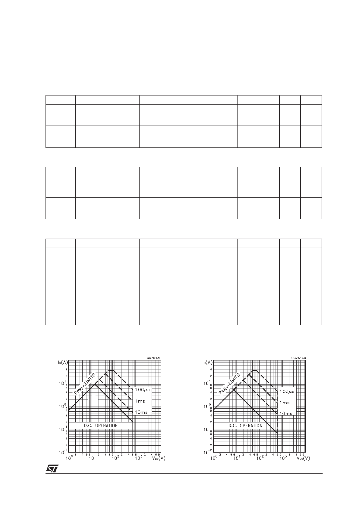
Safe OperatingArea for TO-220 Safe OperatingAreafor TO-220FP
A
A
ns
µC
A
3/9
 Loading...