

SGS Thomson Microelectronics STP8NS25FP, STP8NS25 Datasheet
1/9April 2001
STP8NS25
STP8NS25FP
N-CHANNEL 250V - 0.38Ω - 8A TO-220/TO-220FP
MESH OVERLAY™ MOSFET
■ TYPICAL R
DS
(on) = 0.38 Ω
■ EXTREMELY HIGH dv /d t C APABILITY
■ 100% AVALANCHE TESTED
DESCRIPTION
Using the latest high voltage MESH OVERLAY™
process, STMicroelectronics has designed an advanced family of power MOSFETs with outstanding
performance. The new patented STrip layout coupled with the Company’s proprietary edge termination structure, makes it suitable in coverters for
lighting applications.
APPLICATIONS
■ HIGH CURRENT, HIGH SPEED SWITCHING
■ SWITH MODE POWER SUPPLI ES ( SMPS)
■ DC-DC CONVERTERS FOR TELECOM,
INDUSTRIAL, AND LIGHTING EQUIPMENT
ABSOLUTE MAXIMUM RATINGS
(•)Pu l se width limited by safe operating area
TYPE V
DSS
R
DS(on)
I
D
STP8NS25
STP8NS25F P
250 V
250 V
< 0.45
Ω
< 0.45
Ω
8 A
8 A
Symbol Parameter Value Unit
STP8NS25 STP8NS25FP
V
DS
Drain-source Voltage (VGS = 0)
250 V
V
DGR
Drain-gate Voltage (RGS = 20 kΩ)
250 V
V
GS
Gate- source Voltage ± 20 V
I
D
Drain Current (continuos) at TC = 25°C
8 8(*) A
I
D
Drain Current (continuos) at TC = 100°C
5 5(*) A
I
DM
(●)
Drain Current (pulsed) 32 32(*) A
P
TOT
Total Dissipation at TC = 25°C
80 30 W
Derating Factor 0.64 0.24 W/°C
dv/dt (1) Peak Diode Recovery voltage slope 5 V/ns
V
ISO
Insulation Withstand Voltage (DC) - 2000 V
T
stg
Storage Temperature –65 to 150 °C
T
j
Max. Operating Junction Temperature 150 °C
(1) I
SD
≤
8A, di/dt≤300 A/µs, V
DD
≤
V
(BR)DSS
, Tj≤T
jMAX
(*)Limit ed only by max i mum tempe rat ure allowed
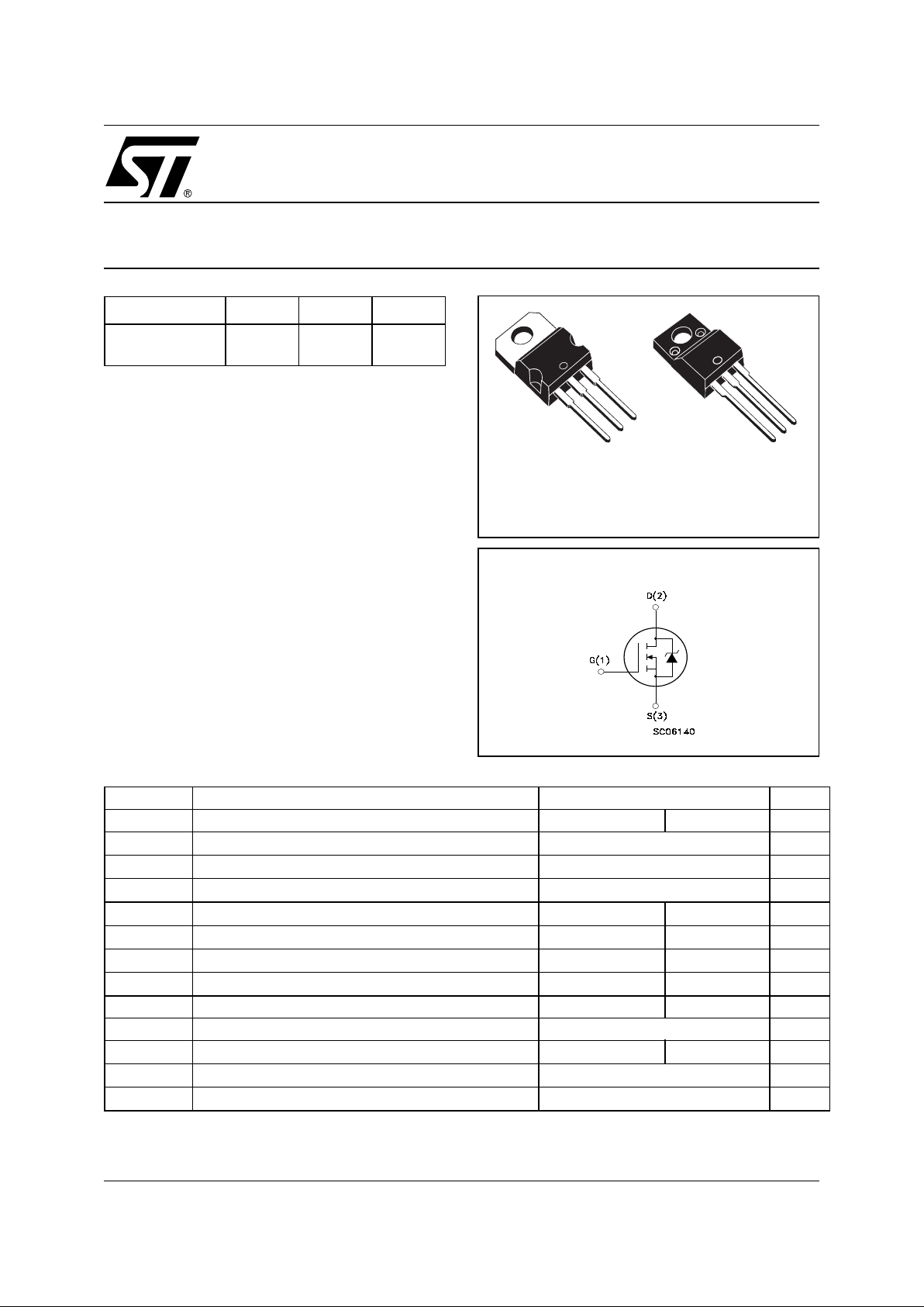
INTERNAL SCHEMATIC DIAGRAM
TO-220
1
2
3
1
2
3
TO-220FP

STP8NS25/STP8NS25FP
2/9
THERMA L D ATA
ELECTRICAL CHARACTERISTICS (TCASE = 25 °C UNLESS OTHERWISE SPECIFIED)
OFF
ON
(1)
DYNAMIC
TO-220 TO-220FP
Rthj-case Thermal Resistance Junction-case Max 1.56 4.11 °C/W
Rthj-amb Thermal Resistance Junction-ambient Max 62.5 °C/W
Rthc-sink Thermal Resistance Case-sink Typ 0.5 °C/W
T
l
Maximum Lead Temperature For Soldering Purpose 300 °C
Symbol Parameter Test Conditions Min. Typ. Max. Unit
V
(BR)DSS
Drain-source
Breakdown Voltage
ID = 250 µA, VGS = 0 250 V
I
DSS
Zero Gate Voltage
Drain Current (V
GS
= 0)
V
DS
= Max Rating
1µA
V
DS
= Max Rating, TC = 125 °C
10 µA
I
GSS
Gate-body Leakage
Current (V
DS
= 0)
V
GS
= ±20V ±100 nA
Symbol Parameter Test Conditions Min. Typ. Max. Unit
V
GS(th)
Gate Threshold Voltage
V
DS
= VGS, ID = 250µA
234V
R
DS(on)
Static Drain-source On
Resistance
VGS = 10V, ID = 4 A
0.38 0.45
Ω
I
D(on)
On State Drain Current VDS > I
D(on)
x R
DS(on)max,
V
GS
=10V
8A
Symbol Parameter Test Conditions Min. Typ. Max. Unit
g
fs
(1) Forward Transconductance VDS > I
D(on)
x R
DS(on)max,
I
D
=4A
78 S
C
iss
Input Capacitance
V
DS
= 25V, f = 1 MHz, VGS = 0
770 pF
C
oss
Output Capacitance 118 pF
C
rss
Reverse Transfer
Capacitance
48 pF
3/9
STP8NS25/STP8NS25FP
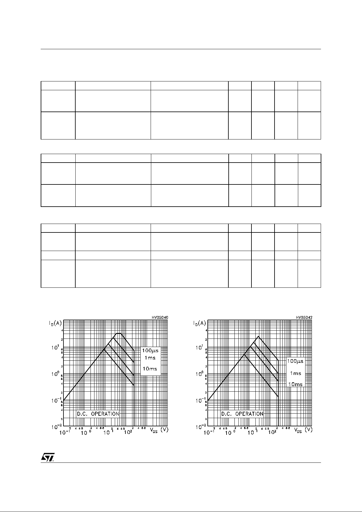
Safe Operating Area for TO-220
ELECTRICAL CHARACTERISTICS (CONTINUED)
SWITCHING ON
SWITCHING OFF
SOURCE DRAIN DIODE
Note: 1. Pulsed: Pu l se duration = 300 µs, duty cycle 1.5 %.
2. Pulse width li mited by safe operating ar ea.
Symbol Parameter Test Conditions Min. Typ. Max. Unit
t
d(on)
Turn-on Delay Time
V
DD
= 125 V, ID = 4 A
RG= 4.7Ω VGS = 10 V
(see test circuit, Figure 3)
13 ns
t
r
Rise Time 18 ns
Q
g
Total Gate Charge
V
DD
= 200V, ID = 8 A,
VGS = 10V
37 51.8 nC
Q
gs
Gate-Source Charge 5.2 nC
Q
gd
Gate-Drain Charge 14.8 nC
Symbol Parameter Test Conditions Min. Typ. Max. Unit
t
d(Voff)
t
f
Turn-off- Delay Time
Fall Time
VDD = 125V, ID = 4 A,
RG=4.7Ω, V
GS
= 10V
(see test circuit, Figure 3)
51
16
ns
ns
t
r(Voff)
t
f
t
c
Off-voltage Rise Time
Fall Time
Cross-over Time
V
clamp
= 200V, ID = 8 A,
R
G
=4.7Ω, V
GS
= 10V
(see test circuit, Figure 5)
12.5
12.5
28
ns
ns
ns
Symbol Parameter Test Conditions Min. Typ. Max. Unit
I
SD
Source-drain Current 8 A
I
SDM
(2)
Source-drain Current (pulsed) 32 A
VSD (1)
Forward On Voltage
ISD = 8 A, VGS = 0
1.7 V
t
rr
Reverse Recovery Time
I
SD
= 8 A, di/dt = 100A/µs
VDD = 30V, Tj = 150°C
(see test circuit, Figure 5)
198 ns
Q
rr
Reverse Recovery Charge 1.1
µ
C
I
RRM
Reverse Recovery Current 11.3 A
Safe Operating Area for TO-220FP
 Loading...