

SGS Thomson Microelectronics STP8NM60FP, STP8NM60, STD5NM60-1 Datasheet
STP8NM60, STP8NM60FP
STD5NM60, STD5NM60-1
N-CHANNEL 600V - 0.9Ω - 8A TO-220/TO-220FP/DPAK/IPAK
MDmesh™ Power MOSF ET
TYPE V
STP8NM60
STP8NM60FP
STD5NM60
STD5NM60-1
■ TYPICAL R
■ HIGH dv/dt AND AVALANCHE CAPABILITIES
■ 100% AVALANCHE TESTED
■ LOW INPUT CAPACITANCE AND GATE
600 V
600 V
600 V
600 V
(on) = 0.9Ω
DS
DSS
R
DS(on)
<1Ω
<1Ω
<1Ω
<1Ω
I
D
8A
8A(*)
5A
5A
Pw
100 W
30 W
96 W
96 W
CHARGE
■ LOW GATE INPUT RESISTANCE
DESCRIPTION
The MDmesh™ is a new revolutionary MOSFET
technology that associates t he Multiple Drain process with the Company’s PowerMESH™ horizontal
layout. Theresulting produc t has an outstanding low
on-resistance, impressively high dv/dt and excellent
avalanche c harac teristics. The adoption of the
Company’s proprietary strip technique yields overall
dynamic perfo rmance that issignificantly better than
that of similar completition’s products.
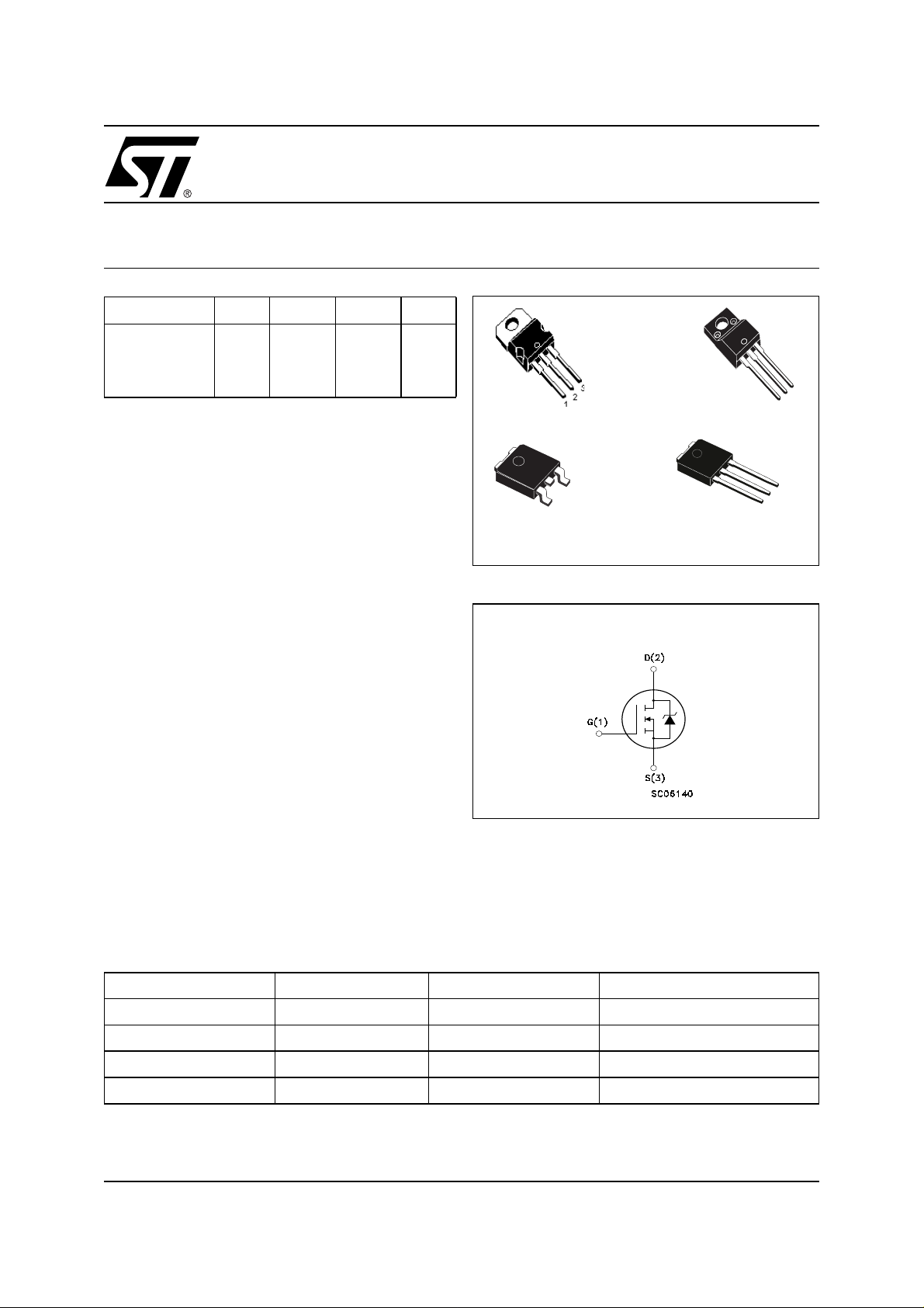
TO-220
3
1
DPAK
TO-252
TO-220FP
IPAK
TO-251
INTERNAL SCHEMATIC DIAGRAM
3
2
1
3
2
1
APPLICATIONS
The MDmesh™ family is very suitable for increase
the power density of high voltage con verters allowing system miniaturization and higher efficiencies.
ORDERING INFORMATION
SALES TYPE MARKING PACKAGE PACKAGING
STP8NM60 P8NM60 TO-220 TUBE
STP8NM60FP P8NM60FP TO-220FP TUBE
STD5NM60T4 D5NM60 DPAK TAPE & REEL
STD5NM60-1 D5NM60 IPAK TUBE
1/13August 2003
STP8NM60, STP8NM60FP, STD5NM60, STD5NM60-1
ABSOLUTE MAXIMUM RATINGS
Symbol Parameter Value Unit
STP8NM60 STP8NM60FP
I
V
DM
P
V
DGR
V
I
I
TOT
DS
GS
D
D
Drain-source Voltage (VGS=0)
Drain-gate Voltage (RGS=20kΩ)
600 V
600 V
Gate- source Voltage ± 30 V
Drain Current (continuous) at TC= 25°C
Drain Current (continuous) at TC= 100°C
()
Drain Current (pulsed) 32 32 (*) 20 A
Total Dissipation at TC= 25°C
8 8 (*) 5 A
5 5 (*) 3.1 A
100 30 96 W
Derating Factor 0.8 0.24 0.4 W/°C
dv/dt (1) Peak Diode Recovery voltage slope 15 15 15 V/ns
V
ISO
T
j
T
stg
() Pulse width limited by safe operating area
≤5A, di/dt ≤400A/µs, VDD≤ V
(1) I
SD
(*) Limited only by maximum temperature allowed
Insulation Withstand Voltage (DC) - 2500 - V
Operating Junction Temperature
Storage Temperature
(BR)DSS,Tj≤TJMAX.
-55 to 150
-55 to 150
THERMAL DATA
TO-220 TO-220FP
Rthj-case Thermal Resistance Junction-case Max 1.25 4.16 1.3 °C/W
Rthj-amb Thermal Resistance Junction-ambient Max 62.5 °C/W
T
l
Maximum Lead Temperature For Soldering Purpose
300 °C
STD5NM60
STD5NM60-1
DPAK
IPAK
°C
°C
AVALANCHE CHARACTERISTICS
Symbol Parameter Max Value Unit
I
AR
E
AS
Avalanche Current, Repetitive or Not-Repetitive
(pulse width limited by T
max)
j
Single Pulse Avalanche Energy
(starting T
= 25 °C, ID=IAR,VDD=50V)
j
ELECTRICAL CHARACTERISTICS (T
=25°C UNLESS OTHERWISE SP ECIFIED)
CASE
2.5 A
200 mJ
ON/OFF
Symbol Parameter Test Conditions Min. Typ. Max. Unit
V
(BR)DSS
V
R
2/13
I
DSS
I
GSS
GS(th)
DS(on)
Drain-source
Breakdown Voltage
Zero Gate Voltage
Drain Current (V
GS
=0)
Gate-body Leakage
Current (V
DS
=0)
Gate Threshold Voltage
Static Drain-source On
Resistance
ID= 250 µA, VGS= 0 600 V
V
= Max Rating
DS
VDS= Max Rating, TC= 125 °C
V
= ± 30V ±100 nA
GS
V
DS=VGS,ID
= 250µA
345V
1
10
VGS=10V,ID= 2.5 A 0.9 1 Ω
µA
µA
STP8NM60, STP8NM60FP, STD5NM60, STD5NM60-1
ELECTRICAL CHARACTERISTICS (T
=25°C UNLESS OTHERWISE SP ECIFIED)
CASE
DYNAMIC
Symbol Parameter Test Conditions Min. Typ. Max. Unit
(1) Forward Transconductance VDS=I
g
fs
D(on)xRDS(on)max,
2.4 S
ID= 2.5A
C
oss eq.
C
iss
C
oss
C
rss
Input Capacitance
Output Capacitance
Reverse Transfer
Capacitance
(2) Equivalent Output
=25V,f=1MHz,VGS= 0 440
V
DS
100
10
VGS=0V,VDS= 0V to 480V 50 pF
Capacitance
R
G
Gate Input Resistance f=1 MHz Gate DC Bias = 0
4 Ω
Test Signal Level = 20mV
Open Drain
SWITCHING ON
Symbol Parameter Test Conditions Min. Typ. Max. Unit
t
d(on)
Turn-on Delay Time
t
r
Rise Time
VDD=300V,ID= 2.5 A
RG= 4.7Ω VGS=10V
14
10
(Resistive Load see, Figure 3)
Q
g
Q
gs
Q
gd
Total Gate Charge
Gate-Source Charge
Gate-Drain Charge
=400V,ID=5A,
V
DD
=10V
V
GS
13
18
5
6
SWITCHING OFF
Symbol Parameter Test Conditions Min. Typ. Max. Unit
t
d(off)
t
r(Voff)
Turn-off Delay Time
t
f
Fall Time
VDD= 300 V, ID= 2.5 A
=4.7ΩVGS=10V
R
G
(Resistive Load see, Figure 3)
= 480V, ID=5A,
t
f
t
c
Fall Time
Cross-over Time
Off-voltage Rise Time
V
DD
RG=4.7Ω, VGS= 10V
(Inductive Load see, Figure 5)
23
10
7
10
17
pF
pF
pF
ns
ns
nC
nC
nC
ns
ns
ns
ns
ns
SOURCE DRAIN DIODE
Symbol Parameter Test Conditions Min. Typ. Max. Unit
I
SD
I
SDM
V
SD
t
rr
Q
rr
I
RRM
t
rr
Q
rr
I
RRM
Note: 1. Pulsed: Pulse duration = 300 µs, duty cycle 1.5 %.
2. Pulse width limited by safe o perating area.
Source-drain Current
(2)
Source-drain Current (pulsed)
(1)
Forward On Voltage
Reverse Recovery Time
Reverse Recovery Charge
Reverse Recovery Current
Reverse Recovery Time
Reverse Recovery Charge
Reverse Recovery Current
ISD= 5 A, VGS=0
I
SD
V
DD
(see test circuit, Figure 5)
I
SD
V
DD
(see test circuit, Figure 5)
= 5 A, di/dt = 100A/µs
=100V,Tj=25°C
= 5 A, di/dt = 100A/µs
=100V,Tj=150°C
300
1950
13
445
3005
13.5
8
32
1.5 V
A
A
ns
µC
A
ns
µC
A
3/13
STP8NM60, STP8NM60FP, STD5NM60, STD5NM60-1
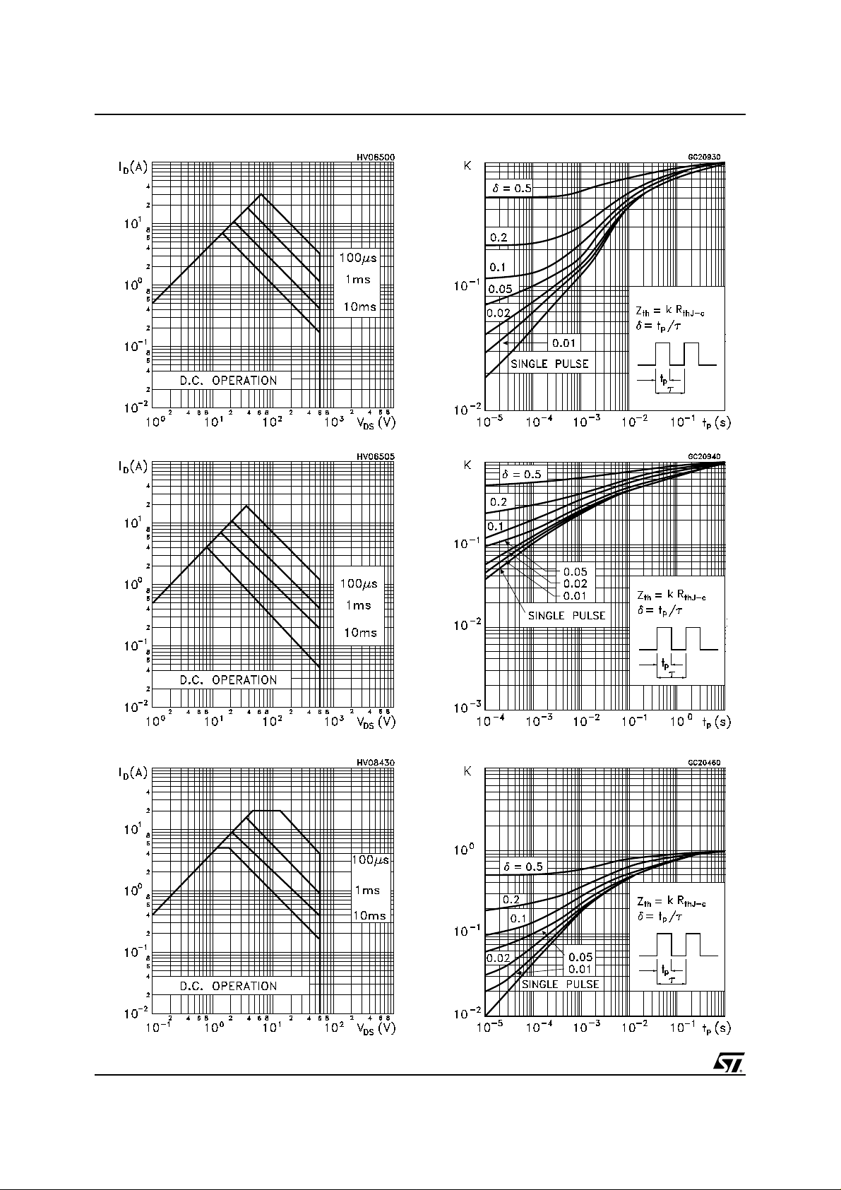
Safe Operating Area For TO-220
Safe Operating Area For TO-220FP
Thermal Impedance For TO-220
Thermal Impedance For TO-220FP
Safe Operating Area For DPAK/IPAK
4/13
Thermal Impedance F or DPAK/IPAK
 Loading...