

1/9
PRELIMINARY DATA
March 2001
STP85NF3LL
STB85NF3LL-1
N-CHANNEL 30V - 0.006Ω - 85A TO -220/I2PAK
LOW GATE CHARGE STripFET™ POWER MOSFET
■ TYPICAL R
DS
(on) = 0.0075 Ω (@4.5V)
■ OPTIMAL R
DS(ON)
x Qg TRADE-OFF @4.5V
■ CONDUCTION LOSSES REDUCED
■ SWITCHING LOSSES REDUCED
DESCRIPTION
This application specific Power MOSFET is the
third genaration of STMicroelectronics unique “
Single Feature Size” strip-based process. The resulting transistor shows the best trade-off between
on-resistance and gate charge. When used as
high and low side in buck regulators, it gives the
best performance in terms of both conduction and
switching losses. This is ext remely important for
motherboards where fast switching and high efficiency are of paramount importance.
APPLICATIONS
■ SPECIFICALL Y D ESIGNED AND OPTIMISED
FOR HIGH EFFICIENCY CPU CORE DC/DC
CONVERTERS
ABSOLUTE MAXIMUM RATINGS
(●) Pulse width limited by safe operating area
TYPE V
DSS
R
DS(on)
I
D
STP85NF3LL
STB85NF3LL-1
30 V
30 V
< 0.008
Ω
< 0.008
Ω
85 A
85 A
Symbol Parameter Value Unit
V
DS
Drain-source Voltage (VGS = 0)
30 V
V
DGR
Drain-gate Voltage (RGS = 20 kΩ)
30 V
V
GS
Gate- source Voltage ± 15 V
I
D
Drain Current (continuos) at TC = 25°C
85 A
I
D
Drain Current (continuos) at TC = 100°C
60 A
I
DM
(●)
Drain Current (pulsed) 340 A
P
TOT
Total Dissipation at TC = 25°C
110 W
Derating Factor 0.73 W/°C
T
stg
Storage Temperature –65 to 175 °C
T
j
Max. Operating Junction Temperature 175 °C
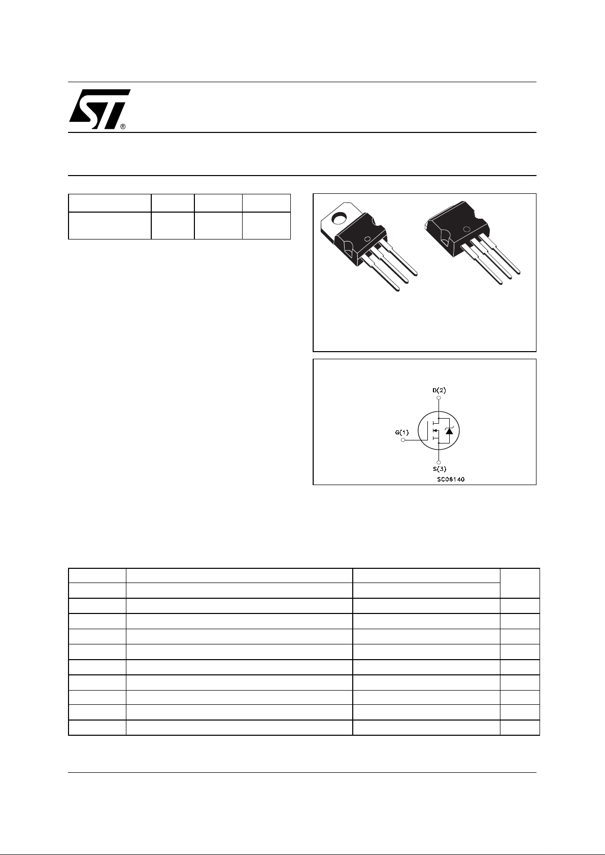
TO-220
1
2
3
1
2
3
I2PAK
INTERNAL SCHEMATIC DIAGRAM
STP85NF3LL/STB85NF3LL-1
2/9
THERMA L D ATA
ELECTRICAL CHARACTERISTICS (TCASE = 25 °C UNLESS OTHERWISE SPECIFIED)
OFF
ON
(1)
DYNAMIC
Rthj-case Thermal Resistance Junction-case Max 1.36 °C/W
Rthj-amb Thermal Resistance Junction-ambient Max 62.5 °C/W
T
l
Maximum Lead Temperature For Soldering Purpose 300 °C
Symbol Parameter Test Conditions Min. Typ. Max. Unit
V
(BR)DSS
Drain-source
Breakdown Voltage
ID = 250 µA, VGS = 0 30 V
I
DSS
Zero Gate Voltage
Drain Current (V
GS
= 0)
V
DS
= Max Rating
1µA
V
DS
= Max Rating, TC = 125 °C
10 µA
I
GSS
Gate-body Leakage
Current (V
DS
= 0)
V
GS
= ± 15V ±100 nA
Symbol Parameter Test Conditions Min. Typ. Max. Unit
V
GS(th)
Gate Threshold Voltage
V
DS
= VGS, ID = 250µA
1V
R
DS(on)
Static Drain-source On
Resistance
VGS = 10V, ID = 40 A
0.006 0.008
Ω
VGS = 4.5V, ID = 40 A
0.0075 0.0095
Ω
Symbol Parameter Test Conditions Min. Typ. Max. Unit
g
fs
(1) Forward Transconductance VDS > I
D(on)
x R
DS(on)max,
ID= 40 A
30 S
C
iss
Input Capacitance
V
DS
= 25V, f = 1 MHz, VGS = 0
2210 pF
C
oss
Output Capacitance 635 pF
C
rss
Reverse Transfer
Capacitance
138 pF
3/9
STP85NF3LL/STB85NF3LL-1
ELECTRICAL CHARACTERISTICS (CONTINUED)
SWITCHING ON
SWITCHING OFF
SOURCE DRAIN DIODE
Note: 1. Pulsed: Pu l se duration = 300 µs, duty c yc l e 1.5 %.
2. Pulse width li mited by safe operating area.
Symbol Parameter Test Conditions Min. Typ. Max. Unit
t
d(on)
Turn-on Delay Time
V
DD
= 15V, ID = 30A
R
G
= 4.7Ω VGS = 4.5V
(see test circuit, Figure 3)
22 ns
t
r
Rise Time 130 ns
Q
g
Q
gs
Q
gd
Total Gate Charge
Gate-Source Charge
Gate-Drain Charge
V
DD
= 24V, ID = 60A,
VGS = 4.5V
30
9
12.5
40 nC
nC
nC
Symbol Parameter Test Conditions Min. Typ. Max. Unit
t
d(off)
t
f
Turn-off-Delay Time
Fall Time
V
DD
= 15V, ID = 30A,
RG=4.7Ω, V
GS
= 4.5V
(see test circuit, Figure 3)
36.5
36.5
ns
ns
t
d(off)
t
f
t
c
Off-voltage Rise Time
Fall Time
Cross-over Time
Vclamp =24V, I
D
=30A
R
G
=4.7Ω, V
GS
= 4.5V
(see test circuit, Figure 5)
32
23
40
ns
ns
ns
Symbol Parameter Test Conditions Min. Typ. Max. Unit
I
SD
Source-drain Current 85 A
I
SDM
(1)
Source-drain Current (pulsed) 340 A
VSD (2)
Forward On Voltage
ISD = 85A, VGS = 0
1.3 V
t
rr
Q
rr
I
RRM
Reverse Recovery Time
Reverse Recovery Charge
Reverse Recovery Current
I
SD
= 85A, di/dt = 100A/µs,
VDD = 15V, Tj = 150°C
(see test circuit, Figure 5)
65
105
3.4
ns
nC
A
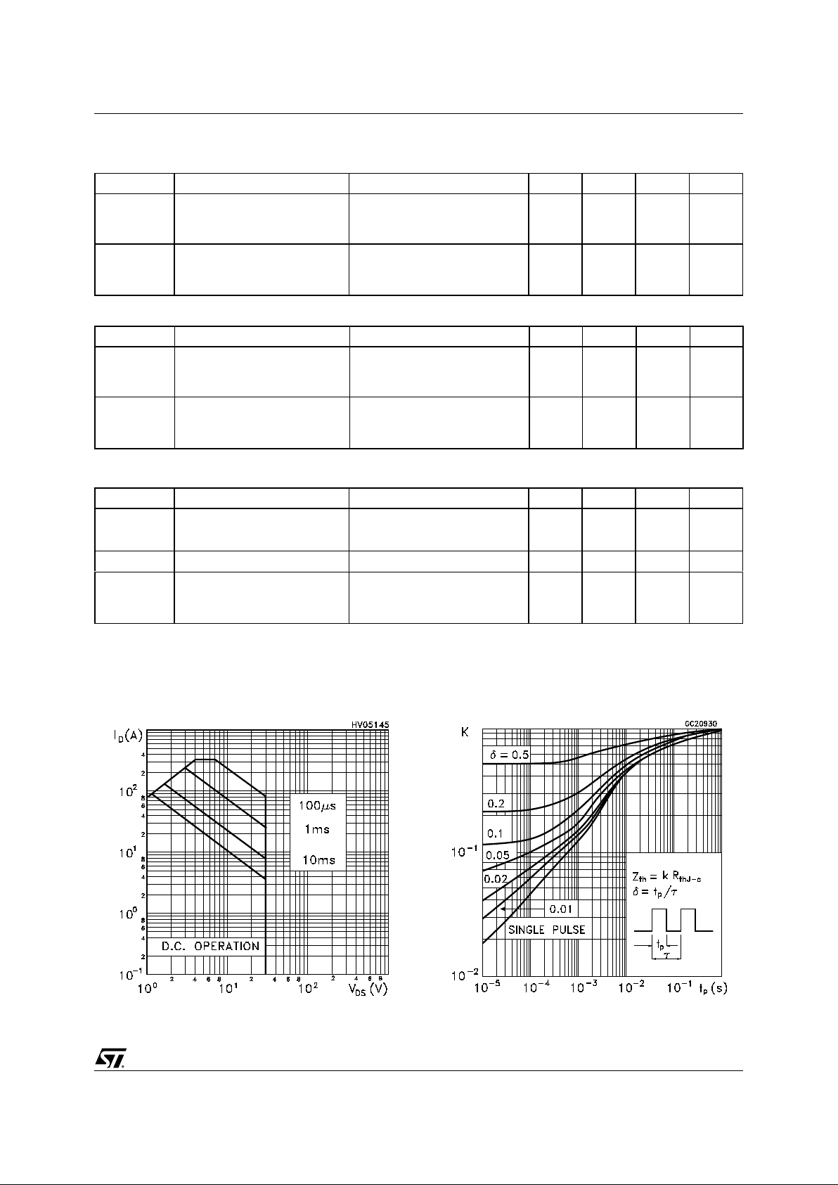
Thermal ImpedenceSafe Operating Area
 Loading...