

SGS Thomson Microelectronics STP80PF55 Datasheet
STP80PF55
P-CHANNEL 55V - 0.016 Ω - 80A TO -220
STripFET™ II POWER MOSFET
PRELIMINARY DATA
TYPE
V
DSS
STB80PF55 55 V < 0.018
■ TYPICAL R
■ EXCEPTIONA L dv/d t CAPABILITY
■ 100% AVALANCHE TESTED
■ APPLICATION ORIENTED
(on) = 0.016 Ω
DS
R
DS(on)
I
D
80 A
Ω
CHARACTERIZATION
DESCRIPTION
This Power MOSFET is the latest dev elo pment of
STMicroelectronis unique "Single Feature Size™"
strip-based process. The resulting transistor
shows extremely high packing density for low onresistance, rugged avalanche characteristics and
less critical alignment steps therefore a remarkable manufacturing reproducibility.
APPLICATIONS
■ MOTOR CONTROL
■ DC-DC & DC-AC CONVERTERS
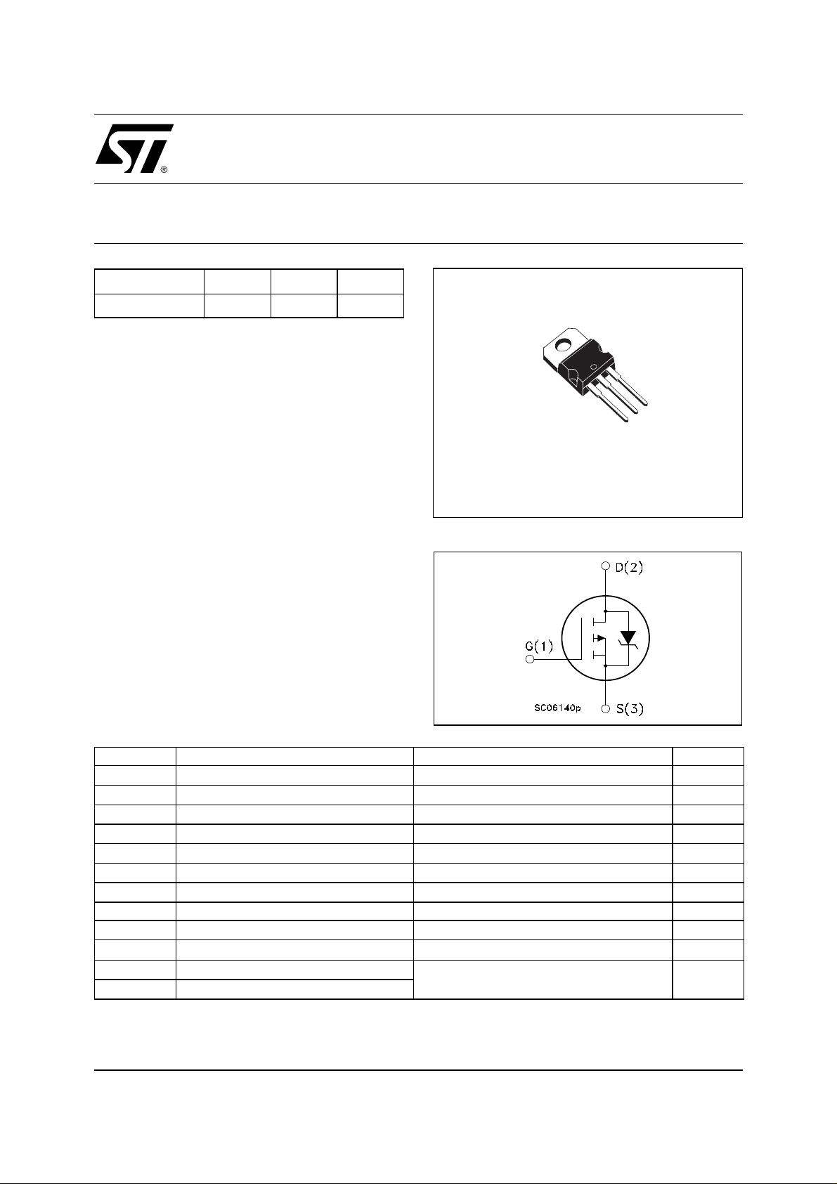
3
2
1
TO-220
INTERNAL SCHEMATIC DIAGRAM
ABSOLUTE MAXIMUM RATINGS
Symbol Parameter Value Unit
V
DS
V
DGR
V
GS
(*) Drain Current (continuos) at T
I
D
I
D
(
I
DM
P
tot
dv/dt
E
AS
T
stg
T
j
(
Pulse widt h l i m i ted by safe op erating area
•)
(*) Curren t Lim i ted by Package
February 2002
This is preliminary information on a new product now in development or undergoing evaluation. Details are subject to change without notice.
Drain-source Voltage (VGS = 0)
Drain-gate Voltage (RGS = 20 kΩ)
55 V
55 V
Gate- source Voltage ± 16 V
= 25°C
C
Drain Current (continuos) at TC = 100°C
•)
Drain Current (pulsed) 320 A
Total Dissipation at TC = 25°C
80 A
57 A
300 W
Derating Factor 2 W/°C
(1)
Peak Diode Recovery voltage slope 7 V/ns
(2)
Single Pulse Avalanche Energy 1.4 mJ
Storage Temperature
Max. Operating Junction Temperature
Note: F or t he P- CHAN NEL MOS FE T ac tu al po la rity o f v olt ages a nd
current has to be rever sed
≤ 40A, di/dt ≤ 300A/µs , VDD ≤ V
(1) I
SD
(2) Starting Tj = 25 oC, ID = 80A, VDD = 40V
-55 to 175 °C
(BR)DSS
, Tj ≤ T
JMAX.
1/6
STP80PF55
THERMA L D ATA
Rthj-case
Rthj-amb
T
Thermal Resistance Junction-case
Thermal Resistance Junction-ambient
Maximum Lead Temperature For Soldering Purpose
l
Max
Max
Typ
0.5
62.5
300
°C/W
°C/W
°C
ELECTRICAL CHARACTERISTICS (T
= 25 °C unless otherwise specified)
case
OFF
Symbol Parameter Test Conditions Min. Typ. Max. Unit
I
V
(BR)DSS
Drain-source
= 250 µA, VGS = 0
D
55 V
Breakdown Voltage
V
= Max Rating
DS
V
= Max Rating TC = 125°C
DS
V
= ± 16 V
GS
1
10
±100 nA
ON
(*)
I
DSS
I
GSS
Zero Gate Voltage
Drain Current (V
GS
Gate-body Leakage
Current (V
DS
= 0)
= 0)
Symbol Parameter Test Conditions Min. Typ. Max. Unit
V
V
GS(th)
R
DS(on)
Gate Threshold Voltage
Static Drain-source On
= VGS ID = 250 µA
DS
V
= 10 V ID = 40 A
GS
234V
0.016 0.018
Resistance
DYNAMIC
Symbol Parameter Test Conditions Min. Typ. Max. Unit
> I
g
fs
C
iss
C
oss
C
rss
Forward Transconductance
Input Capacitance
Output Capacitance
Reverse Transfer
Capacitance
V
DS
I
D
V
DS
= 40 A
x R
D(on)
DS(on)max,
= 25V, f = 1 MHz, VGS = 0
32 S
5500
1130
600
µA
µA
Ω
pF
pF
pF
2/6
 Loading...