

SGS Thomson Microelectronics STP80NF55L-06 Datasheet
STP80NF55L-06
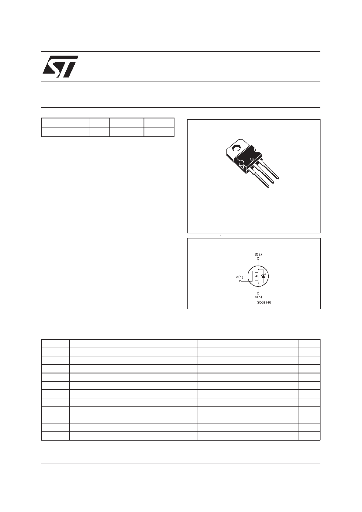
N - CHANNEL 55V - 0.005 Ω - 80A TO-220
STripFET POWER MOSFET
TYPE V
DSS
R
DS(on)
I
D
ST P80NF55L-06 55 V < 0.006 5 Ω 80 A
■ TYPICALR
■ LOW THRESHOLDDRIVE
■ LOGICLEVEL DEVICE
DS(on)
= 0.005 Ω
DESCRIPTION
This PowerMOSFET is the latest developmentof
STMicroelectronics unique ”Single Feature
Size” strip-based process. The resulting
transistor shows extremely high packing density
for low on-resistance, rugged avalanche
characteristics and less critical alignment steps
therefore a remarkable manufacturing
reproducibility.
APPLICATIONS
■ HIGHCURRENT, HIGH SPEED SWITCHING
■ SOLENOIDAND RELAYDRIVERS
■ MOTORCONTROL, AUDIO AMPLIFIERS
■ DC-DC& DC-ACCONVERTERS
3
2
1
TO-220
INTERNAL SCHEMATIC DIAGRAM
ABSOLUTE MAXIMUM RATINGS
Symbol Parameter Value Uni t
V
V
V
I
DM
P
E
AS
T
(•) Pulse width limitedby safe operating area (1) starting Tj
October 1999
Dra in- sour c e Volta ge (VGS=0) 55 V
DS
Drain- gate Voltage (RGS=20kΩ)55V
DGR
Gate-s ource Volt age ± 20 V
GS
Dra in Cu rr ent (continuous) at Tc=25oC80A
I
D
Dra in Cu rr ent (continuous) at Tc= 100oC57A
I
D
(
Dra in Cu rr ent (pulsed) 320 A
•)
Tot al Dissi pat io n at Tc=25oC 210 W
tot
Der ati ng Fa c t or 1.4 W/
(1) Single Pu lse Avalanche E n ergy 1 J
St orage Tem pe ra t ure -65 to 175
stg
Max. Operating Junction Tem pe ra t ure 175
T
j
=25oC,ID=40A , VDD= 30V
o
C
o
C
o
C
1/8
STP80NF55L-06
THERMAL DATA
R
thj-case
R
thj-amb
T
Ther mal Resistanc e Junct ion-case Max
Ther mal Resistanc e Junct ion-ambient Max
Maximum L ead Temperature For So ldering Purpos e
l
0.71
62.5
300
o
C/W
o
C/W
o
C
ELECTRICAL CHARACTERISTICS
=25oC unless otherwisespecified)
(T
case
OFF
Symbol Parameter Test Conditions Min. Typ. Max. U nit
V
(BR)DSS
Drain-source
ID=250µAVGS=0 55 V
Break dow n Vo lt age
I
DSS
I
GSS
Zero Gate Voltage
Drain Curre nt (V
GS
Gat e- bod y Leakag e
Current (V
DS
=0)
=0)
V
=MaxRating
DS
=MaxRating Tc=125oC
V
DS
V
= ± 20 V ± 100 nA
GS
1
10
ON(∗)
Symbol Parameter Test Conditions Min. Typ. Max. U nit
V
GS(th)
R
DS(on)
I
D(on)
Gate Threshold Voltage VDS=VGSID= 250 µ A11.62.5V
Sta t ic Drain-s our c e On
Resistance
On State Drain Current VDS>I
VGS=10V ID=40A
V
=5V ID=40A
GS
D(on)xRDS(on )max
0.005
0.0055
0.0065
0.008
80 A
VGS=10V
DYNAMIC
Symbol Parameter Test Conditions Min. Typ. Max. U nit
g
(∗)Forward
fs
Tr ansc on duc tance
C
C
C
Input Capaci t ance
iss
Out put Capac itance
oss
Reverse Transfer
rss
Capacit a nc e
VDS>I
D(on)xRDS(on )maxID
=18 A 20 S
VDS=25V f=1MHz VGS= 0 7600
990
270
µA
µ
Ω
Ω
pF
pF
pF
A
2/8
STP80NF55L-06
ELECTRICAL CHARACTERISTICS
(continued)
SWITCHINGON
Symbol Parameter Test Conditions Min. Typ. Max. U nit
t
d(on)
Tur n-on Delay Time
Rise Time
t
r
VDD=27V ID=40A
R
=4.7
G
Ω
VGS=4.5V
75
300
(Resis t iv e Load, see fig. 3)
Q
Q
Q
Tot al Gate Charge
g
Gat e- Source Char g e
gs
Gate-Drain Charge
gd
VDD=44V ID=80A VGS=5V 97
25
46
100 nC
SWITCHINGOFF
Symbol Parameter Test Conditions Min. Typ. Max. U nit
t
d(off)
Tur n-of f Dela y Tim e
t
Fall T ime
f
VDD=27V ID=40A
=4.7 Ω VGS=4.5V
R
G
210
160
(Resis t iv e Load, see fig. 3)
t
d(off)
Off-volt age Rise Time
t
Fall T ime
f
t
Cross-over Tim e
c
Vclamp = 44 V ID=80A
=4.7 Ω VGS=4.5V
R
G
(Indu ct iv e Load, see fig . 5)
90
230
350
SOURCEDRAIN DIODE
Symbol Parameter Test Conditions Min. Typ. Max. U nit
I
V
I
SDM
SD
Q
I
RRM
SD
t
Source-drain Current
(•)
Source-drain Current
80
320
(pulsed)
(∗)ForwardOnVoltage ISD=80A VGS=0 1.5 V
Reverse Recovery
rr
Time
Reverse Recovery
rr
ISD= 80 A di/dt = 100 A /µs
=25V Tj=150oC
V
DD
(see test circuit, fig. 5)
75
190
Charge
Reverse Recovery
5.1
Current
ns
ns
nC
nC
ns
ns
ns
ns
ns
A
A
ns
nC
A
(∗) Pulsed: Pulse duration = 300 µs, duty cycle 1.5%
(•) Pulse width limited by safeoperating area
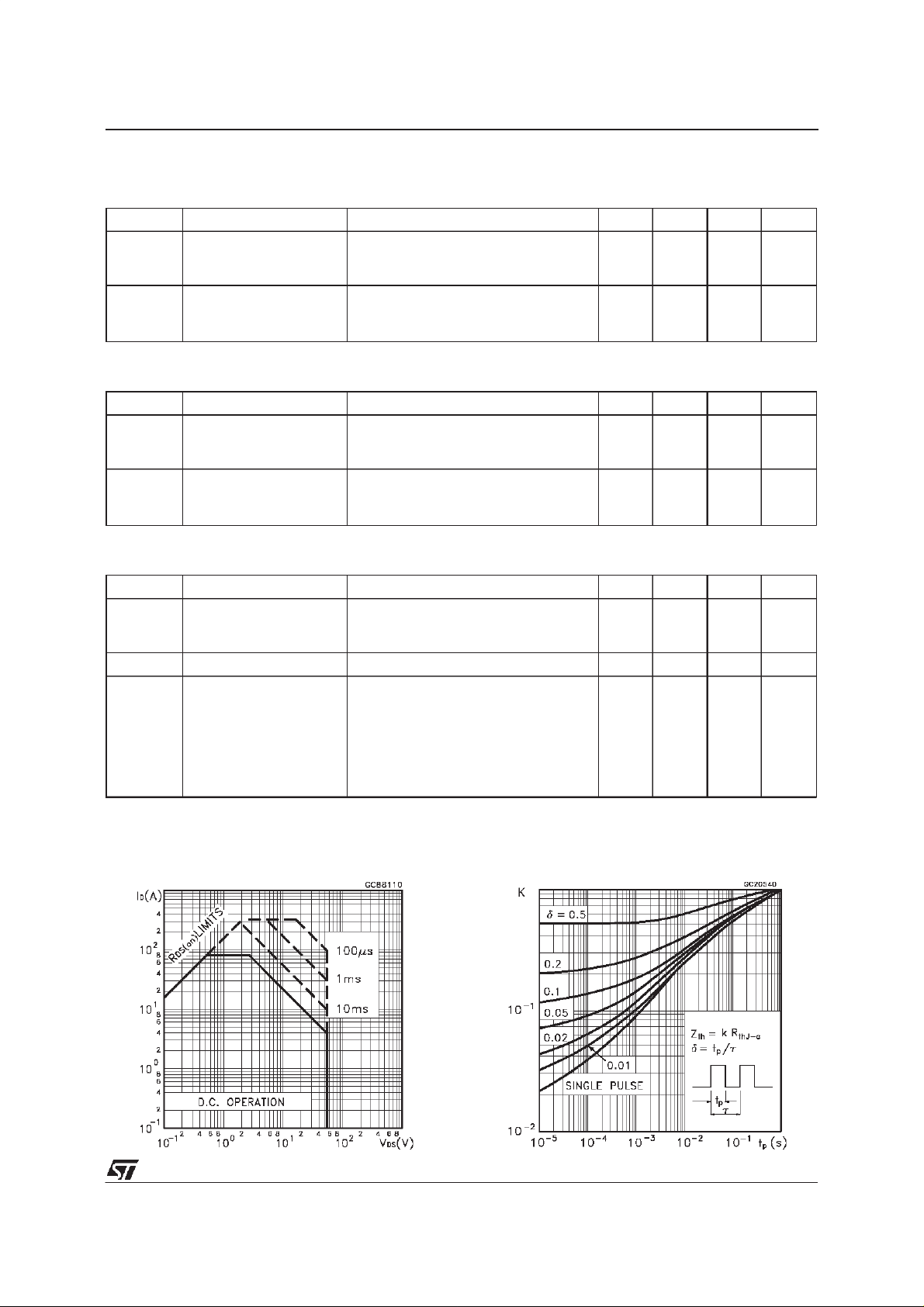
SafeOperating Area ThermalImpedance
3/8
 Loading...