

SGS Thomson Microelectronics STP80NF55-06FP, STP80NF55-06 Datasheet
STP80NF55-06
N - CHANNEL 55V - 0.005Ω - 80A TO-220/TO-220FP
TYPE V
ST P80NF55-06
ST P80NF55-06FP
■ TYPICALR
■ EXCEPTIONALdv/dtCAPABILITY
■ 100%AVALANCHETESTED
■ APPLICATIONORIENTED
DS(on)
DSS
55 V
55 V
= 0.005
CHARACTERIZATION
DESCRIPTION
This Power Mosfet is the latest development of
STMicroelectronics unique ”Single Feature
Size ” strip-based process. The resultingtransi-
stor shows extremelyhigh packing density forlow
on-resistance, rugged avalance characteristics
and less critical alignment steps therefore a remarkablemanufacturingreproducibility.
APPLICATIONS
■ SOLENOIDAND RELAY DRIVERS
■ MOTORCONTROL, AUDIOAMPLIFIERS
■ DC-DCCONVERTERS
■ AUTOMOTIVEENVIRONMENT
R
DS(on)
< 0.0065 Ω
< 0.0065
Ω
I
D
80 A
60 A
Ω
STP80NF55-06FP
STripFET POWER MOSFET
PRELIMINARY DATA
3
2
1
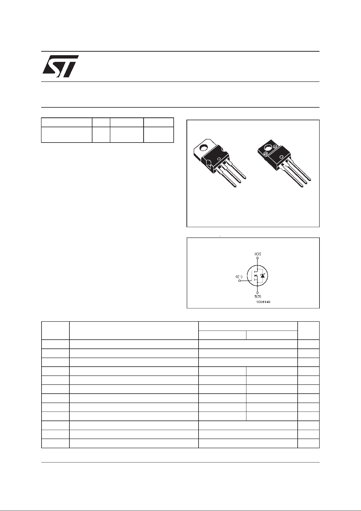
TO-220 TO-220FP
INTERNAL SCHEMATIC DIAGRAM
3
2
1
ABSOLUTE MAXIMUM RATINGS
Symbol Parameter Value Uni t
ST P80NF55-06 ST P55NF 55- 06F P
V
V
V
I
DM
P
V
dv/ dt Peak Diode Recov er y voltage sl ope 7 V/ n s
T
(•) Pulsewidth limited by safe operating area (1)ISD≤ 80 A, di/dt ≤ 300 A/µs, VDD≤ V
July 1999
Dra in- sour c e V ol t age (VGS=0) 55 V
DS
Dra in- gate Voltage (RGS=20kΩ)
DGR
Gat e-sourc e Volt age
GS
I
Dra in Curr ent (continuous) at Tc=25oC8060A
D
I
Dra in Curr ent (continuous) at Tc=100oC57 42A
D
55 V
20 V
±
(•) Dr a in Curr ent (pulsed) 320 240 A
Tot al Dissipation at Tc=25oC21050W
tot
Der ati ng F actor 1.43 0.33 W/
Insulation Withstand Voltage (DC)
ISO
St orage Temper at ur e -65 to 175
stg
T
Max. Oper at ing Junc t ion Temperat ur e 175
j
2000 V
(BR)DSS,Tj≤TJMAX
o
C
o
C
o
C
1/6
STP80NF55-06/FP
THERMAL DATA
TO-220 TO-220FP
R
thj-case
R
thj-amb
R
thc-sink
T
AVALANCHE CHARACTERISTICS
Symbol Parameter Max V alue Unit
I
AR
E
Ther mal Resistanc e Junct ion-case Max 0.7 3
Ther mal Resistanc e Junct ion-ambie nt Max
Ther mal Resistanc e Case-sink Ty p
Maximum Lead Temperat ur e F or Soldering Purp os e
l
Avalanche C urrent, Repetitive or Not-Repetitive
(pulse width limited by T
Single Puls e Avalan c he Ener gy
AS
(starting T
=25oC, ID=IAR,VDD=30V)
j
max)
j
62.5
0.5
300
80 A
650 mJ
o
C/W
o
C/W
o
C/W
o
C
ELECTRICAL CHARACTERISTICS
=25oC unless otherwisespecified)
(T
case
OFF
Symbol Parameter Test Conditions Min. Typ. M ax. Unit
V
(BR)DSS
Drain-source
=250µAVGS=0
I
D
55 V
Break dow n Vo lt age
I
DSS
I
GSS
Zero Gate Voltage
Drain Curre nt (V
GS
Gat e- bod y Leakag e
Current (V
DS
=0)
=0)
V
=MaxRating
DS
=MaxRating Tc=125oC
V
DS
=± 20 V
V
GS
1
10
± 100 nA
ON (∗)
Symbol Parameter Test Conditions Min. Typ. M ax. Unit
V
GS(th)
R
DS(on)
Gate Threshold Voltage
Sta t ic Drain-source On
V
DS=VGSID
= 250µA
VGS=10V ID= 40 A 0.005 0.0065 Ω
234V
Resistance
I
D(on)
On State Drain Current VDS>I
D(on)xRDS(on)max
80 A
VGS=10V
DYNAMIC
Symbol Parameter Test Conditions Min. Typ. M ax. Unit
g
(∗)Forward
fs
Tr ansc on duc tance
C
C
C
Input Capacit anc e
iss
Out put Capacit ance
oss
Reverse Transfer
rss
Capacit a nc e
VDS>I
D(on)xRDS(on)maxID
=40 A 50 S
VDS=25V f=1MHz VGS= 0 8000
1100
220
µ
µA
pF
pF
pF
A
2/6
 Loading...