

SGS Thomson Microelectronics STW80NF12, STP80NF12FP, STP80NF12, STB80NF12 Datasheet

1/12March 2003
STB80NF12 STW80NF12
STP80NF12 STP80NF12FP
N-CHANNEL 120V-0.013Ω-80A TO-220/TO-247/TO-2 20FP/D²PAK
STripFET™ II POWER MOSFET
■ TYPICAL R
DS
(on) = 0.013Ω
■ EXCEPTIONAL dv /d t CAPABILITY
■ 100% AVALANCHE TESTED
■ APPLICATION ORIENTED
CHARACTERIZATION
■ SURFACE-MOUNTING D
²
PAK (TO-263)
POWER PACKAG E IN TU BE (NO SU FFIX) OR
IN TAPE & REEL (SUFFIX “T4”)
DESCRIPTION
This MOSFET series realized with STMicroelectronics
unique STripFET process has specifically been designed
to minimize input capacitance and gate charge. It is
therefore suitable as primary switch in advanced highefficiency, high-frequency isolate d DC-DC c onverters for
Telecom and Computer a pplications. It is also intended
for any applications with low gate drive requirements.
APPLICATIONS
■ HIGH-EFFICIENCY DC-DC CONVERTERS
■ UPS AND MOTOR CONTROL
TYPE
V
DSS
R
DS(on)
I
D
STB80NF12
STP80NF12
STP80NF12FP
STW80NF12
120 V
120 V
120 V
120 V
<0.018
Ω
<0.018
Ω
<0.018
Ω
<0.018
Ω
80 A(*)
80 A(*)
80 A(*)
80 A(*)
1
2
3
1
3
1
2
3
TO-220
D²PAK
TO-263
(Suffix “T4”)
TO-220FP
TO-247
ABSOLUTE MAXIMUM RATINGS
(
•)
Pulse widt h l i m i ted by safe operating area.
(*) Limited by Package
(2) I
SD
≤35A, di/dt ≤300A/ µ s , VDD ≤ V
(BR)DSS
, Tj ≤ T
JMAX.
(#) Refer to SOA for the max allovable currente values on FP-type
due to thermal resistance value.
(1) Starting T
j
= 25 oC, ID = 40A, VDD = 45V
Symbol Parameter Value Unit
STB_P_W80NF12 STP80NF12FP
V
DS
Drain-source Voltage (VGS = 0)
120 V
V
DGR
Drain-gate Voltage (RGS = 20 kΩ)
120 V
V
GS
Gate- source Voltage ± 20 V
I
D
(*) Drain Current (continuous) at TC = 25°C
80 80(#) A
I
D
Drain Current (continuous) at TC = 100°C
60 60(#) A
I
DM
(
•)
Drain Current (pulsed) 320 320(#) A
P
tot
Total Dissipation at TC = 25°C
300 45 W
Derating Factor 2.0 0.3 W/°C
dv/dt
(1)
Peak Diode Recovery voltage slope 10 V/ns
E
AS
(2)
Single Pulse Avalanche Energy 700 mJ
V
ISO
Insulation Withstand Voltage (DC) ------ 2500 V
T
stg
Storage Temperature
-55 to 175 °C
T
j
Operating Junction Temperature
INTERNAL SCHEMATIC DIAGRAM
STB80NF12 STW80NF12 STP80NF12 STP80NF12FP
2/12
THERMA L D ATA
ELECTRICAL CHARACTERISTICS (T
case
= 25 °C unless otherwise specified)
OFF
ON
(1)
DYNAMIC
TO-247
D
2
PAK
TO-220
TO-220FP
Rthj-case Thermal Resistance Junction-case Max 0.5 0.5 3.33 °C/W
Rthj-amb
T
l
Thermal Resistance Junction-ambient
Maximum Lead Temperature For Soldering Purpose
Max 50
300
62.5
300
62.5
300
°C/W
°C
Symbol Parameter Test Conditions Min. Typ. Max. Unit
V
(BR)DSS
Drain-source
Breakdown Voltage
I
D
= 250 µA, VGS = 0
120 V
I
DSS
Zero Gate Voltage
Drain Current (V
GS
= 0)
V
DS
= Max Rating
V
DS
= Max Rating TC = 125°C
1
10
µA
µA
I
GSS
Gate-body Leakage
Current (V
DS
= 0)
V
GS
= ± 20V
±100 nA
Symbol Parameter Test Conditions Min. Typ. Max. Unit
V
GS(th)
Gate Threshold Voltage
V
DS
= VGS I
D
= 250 µA
2V
R
DS(on)
Static Drain-source On
Resistance
V
GS
= 10 V ID = 40 A
0.013 0.018
Ω
Symbol Parameter Test Conditions Min. Typ. Max. Unit
g
fs
(*)
Forward Transconductance
V
DS
= 15 V ID = 40 A
80 S
C
iss
C
oss
C
rss
Input Capacitance
Output Capacitance
Reverse Transfer
Capacitance
V
DS
= 25V f = 1 MHz VGS = 0
4300
600
230
pF
pF
pF
3/12
STB80NF12 STW80NF12 STP80N F12 STP80NF12FP
SWITCHING ON
SWITCHING OFF
SOURCE DRAIN DIODE
(*)
Pulsed: P ul se duration = 300 µs, duty cycle 1.5 %.
(
•)Pulse width limited by saf e operating area.
Symbol Parameter Test Conditions Min. Typ. Max. Unit
t
d(on)
t
r
Turn-on Delay Time
Rise Time
V
DD
= 50 V ID = 40 A
R
G
= 4.7 Ω VGS = 10 V
(Resistive Load, Figure 3)
40
145
ns
ns
Q
g
Q
gs
Q
gd
Total Gate Charge
Gate-Source Charge
Gate-Drain Charge
V
DD
= 80 V ID= 80 A VGS= 10V
140
23
51
189 nC
nC
nC
Symbol Parameter Test Conditions Min. Typ. Max. Unit
t
d(off)
t
f
Turn-off Delay Time
Fall Time
V
DD
= 50 V ID = 40 A
R
G
= 4.7Ω, V
GS
= 10 V
(Resistive Load, Figure 3)
134
115
ns
ns
Symbol Parameter Test Conditions Min. Typ. Max. Unit
I
SD
I
SDM
(•)
Source-drain Current
Source-drain Current (pulsed)
80
320
A
A
V
SD
(*)
Forward On Voltage
I
SD
= 80 A VGS = 0
1.3 V
t
rr
Q
rr
I
RRM
Reverse Recovery Time
Reverse Recovery Charge
Reverse Recovery Current
I
SD
= 80 A di/dt = 100A/µs
V
DD
= 35 V Tj = 150°C
(see test circuit, Figure 5)
155
0.85
11
ns
nC
A
ELECTRICAL CHARACTERISTICS (continued)
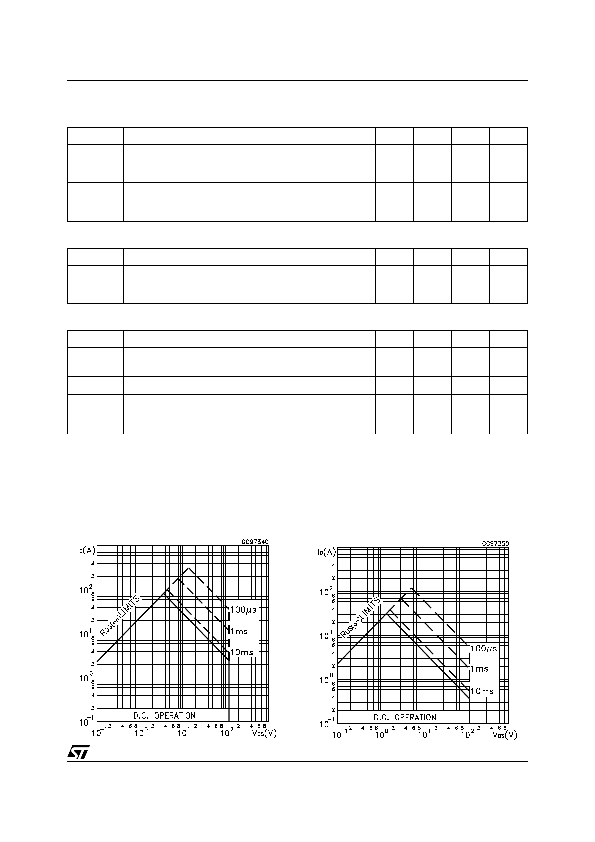
Safe Operating Area Safe Operating Area for TO-220FP

STB80NF12 STW80NF12 STP80NF12 STP80NF12FP
4/12
Thermal Impedance Thermal Impedance for TO-220FP
Output Characteristics Transfer Characteristics
Transconductance Static Drain-source On Resistance
 Loading...