

SGS Thomson Microelectronics STP7NB80FP, STP7NB80 Datasheet
STP7NB80
N - CHANNEL 800V - 1.2Ω - 6.5A - TO-220/TO-220FP
TYPE V
STP7NB80
STP7NB80 FP
■ TYPICALR
■ EXTREMELYHIGH dv/dt CAPABILITY
■ 100%AVALANCHETESTED
■ VERYLOW INTRINSIC CAPACITANCES
■ GATECHARGE MINIMIZED
DS(on)
DSS
800 V
800 V
= 1.2
DESCRIPTION
Using the latest high voltage MESH OVERLAY
process, STMicroelectronics has designed an
advanced family of power MOSFETs with
outstanding performances. The new patent
pending strip layout coupled with the Company’s
proprietary edge termination structure, gives the
lowest RDS(on) per area, exceptional avalanche
and dv/dt capabilities and unrivalled gate charge
and switching characteristics.
Ω
R
DS(on)
<1.5Ω
<1.5
Ω
I
D
6.5 A
6.5 A
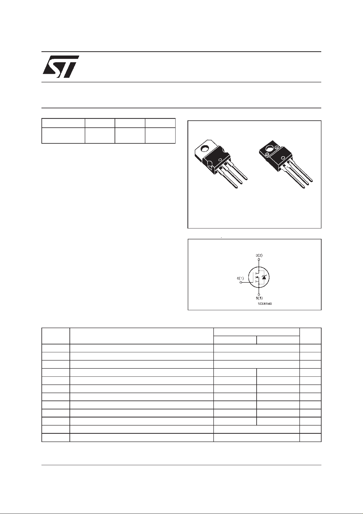
STP7NB80FP
PowerMESH MOSFET
3
2
1
TO-220 TO-220FP
INTERNAL SCHEMATIC DIAGRAM
3
2
1
APPLICATIONS
■ HIGHCURRENT, HIGHSPEEDSWITCHING
■ SWITCHMODE POWER SUPPLIES(SMPS)
■ DC-AC CONVERTERS FOR WELDING
EQUIPMENTAND UNINTERRUPTIBLE
POWERSUPPLIESAND MOTORDRIVE
ABSOLUTE MAXIMUM RATINGS
Symbol Parameter Value Unit
ST P7 NB80 STP 7NB 80FP
V
V
V
I
DM
P
dv/ dt(
V
T
(•) Pulsewidth limited by safe operatingarea (1)ISD≤ 6.5A, di/dt ≤ 200 A/µs,VDD≤ V
*) Limitedonly maximumtemperature allowed
(
April 1999
Drain-sour ce Voltage (VGS=0) 800 V
DS
Drain- ga t e V olt a ge (RGS=20kΩ)
DGR
Gate-sourc e Voltage ± 30 V
GS
Drain C ur r ent (c on t in uous) at Tc=25oC6.56.5(*)A
I
D
Drain C ur r ent (c on t in uous) at Tc= 100oC4.14.1(*)A
I
D
800 V
(•) Drain C ur r ent (pulsed) 26 26 A
Total Dissipation at Tc=25oC 135 40 W
tot
Derating F actor 1.08 0.32 W/
1) Peak Diode Rec o very volt ag e slope 4.5 4.5 V/ns
Ins ulation W i th s tand Voltag e (DC) -- 2000
ISO
Sto rage T e m pe r ature -65 to 1 50
stg
Max. O pe rating Junction T em p er a t ure 150
T
j
(BR)DSS
,Tj≤T
JMAX
o
C
o
C
o
C
o
C
1/9

STP7NB80/FP
THERMAL DATA
TO-220 TO-220FP
R
thj-case
R
thj-amb
R
thc-sink
T
AVALANCHE CHARACTERISTICS
Symbol Para meter Max Val ue Uni t
I
AR
E
Ther mal Resis t an ce Junc ti on-cas e Max 0.92 3.13
Ther mal Resis t an ce Junc ti on-ambien t Ma x
Thermal Resistance Case-sink Typ
Maximum Le ad Temper at u r e For Sold er ing Purpos e
l
Avalanche Cu r rent, Repetitive or No t- Re petitiv e
(pulse width limite d by T
Single Pu lse Avalanche Energy
AS
(starting T
=25oC, ID=IAR,VDD=50V)
j
max)
j
62.5
0.5
300
6.5 A
400 mJ
o
C/W
o
C/W
o
C/W
o
C
ELECTRICAL CHARACTERISTICS
=25oC unless otherwisespecified)
(T
case
OFF
Symbol Parameter Test Conditions Min. Typ. Max. Unit
V
(BR)DSS
Drain-sourc e
=250µAVGS=0
I
D
800 V
Break d own Voltage
I
DSS
I
GSS
Zero Gate Voltage
Drain Current (V
GS
Gat e- b ody Leakage
Current (V
DS
=0)
=0)
V
=MaxRating
DS
= Max Rating Tc=125oC
V
DS
=± 30 V
V
GS
1
50
± 100 nA
ON(∗)
Symbol Parameter Test Conditions Min. Typ. Max. Unit
V
GS(th)
Gate Threshold
V
DS=VGSID
= 250µA
345V
Voltage
R
DS(on)
Static Drain-source O n
VGS=10V ID= 3.2 A 1.2 1.5 Ω
Resistanc e
I
D(on)
On State Drain Cu r rent VDS>I
D(on)xRDS(on)max
6.5 A
VGS=10V
DYNAMIC
Symbol Parameter Test Conditions Min. Typ. Max. Unit
g
(∗)Forward
fs
Tr ansconduc tance
C
C
C
Input Capacit ance
iss
Out put Ca pacita nce
oss
Reverse T ransfer
rss
Capacitance
VDS>I
D(on)xRDS(on)maxID
=3.2A 1.5 6.5 S
VDS=25V f=1MHz VGS= 0 1400
180
20
µ
µA
pF
pF
pF
A
2/9

STP7NB80/FP
ELECTRICAL CHARACTERISTICS
(continued)
SWITCHING ON
Symbol Parameter Test Conditions Min. Typ. Max. Unit
t
d(on)
Turn-on Time
t
r
Rise Tim e
VDD= 400 V ID=3.5A
=4.7 Ω VGS=10V
R
G
20
10
(see t est circuit, fi gure 3)
Q
Q
Q
Total Gate Charge
g
Gat e- Source Charge
gs
Gate-Drain Ch arge
gd
VDD= 640 V ID=7A VGS=10V
=4.7 Ω
R
G
40
10
18
52 nC
SWITCHING OFF
Symbol Parameter Test Conditions Min. Typ. Max. Unit
t
r(Voff)
t
t
Off -voltage R ise Time
Fall Time
f
Cross-ov er T ime
c
VDD= 640 V ID=7A
=4.7 Ω VGS=10V
R
G
(see t est circuit, fi gure 5)
15
15
25
SOURCEDRAINDIODE
Symbol Parameter Test Conditions Min. Typ. Max. Unit
I
SD
I
SDM
V
SD
t
Q
I
RRM
(∗) Pulsed: Pulse duration = 300 µs, duty cycle 1.5 %
(•) Pulse width limited by safe operatingarea
Source-drain C urrent
(•)
Source-drain C urrent
6.5
26
(pulsed)
(∗) Forwar d O n V oltage ISD=6.5A VGS=0 1.6 V
Reverse Recover y
rr
Time
Reverse Recover y
rr
= 7 A di/d t = 100 A/µs
I
SD
= 100 V Tj=150oC
V
DD
(see t est circuit, fi gure 5)
750
7.10
Charge
Reverse Recover y
19
Current
ns
ns
nC
nC
ns
ns
ns
A
A
ns
µ
A
C
SafeOperating Area for TO-220 SafeOperating Area for TO-220FP
3/9
 Loading...