SGS Thomson Microelectronics STP7NB40FP, STP7NB40 Datasheet

N - CHANNEL ENHANCEMENT MODE
TYPE V
STP7NB40
STP7NB40FP
■ TYPICAL R
■ EXTREMELY HIGH dV/dt C A PA BI LIT Y
■ 100% AVALANCHE TESTED
■ VERY LOW INTRINSIC CAPACITANCES
■ GATE CHARGE MINIMIZED
DS(on)
DSS
400 V
400 V
= 0.75 Ω
DESCRIPTION
Using the latest high voltage MESH OVERLAY
process, SGS-Thomson has designed an
advanced family of power MOSFETs with
outstanding performances. The new patent
pending strip layout coupled with the Company’s
proprietary edge termination structure, gives the
lowest RDS(on) per area, exceptional avalanche
and dv/dt capabilities and unrivalled gate charge
and switching char acteristics.
R
DS(on)
< 0.9 Ω
< 0.9 Ω
I
D
7.0 A
4.4 A
STP7NB40
STP7NB40FP
PowerMESH MOSFET
PRELIMINARY DATA
3
2
1
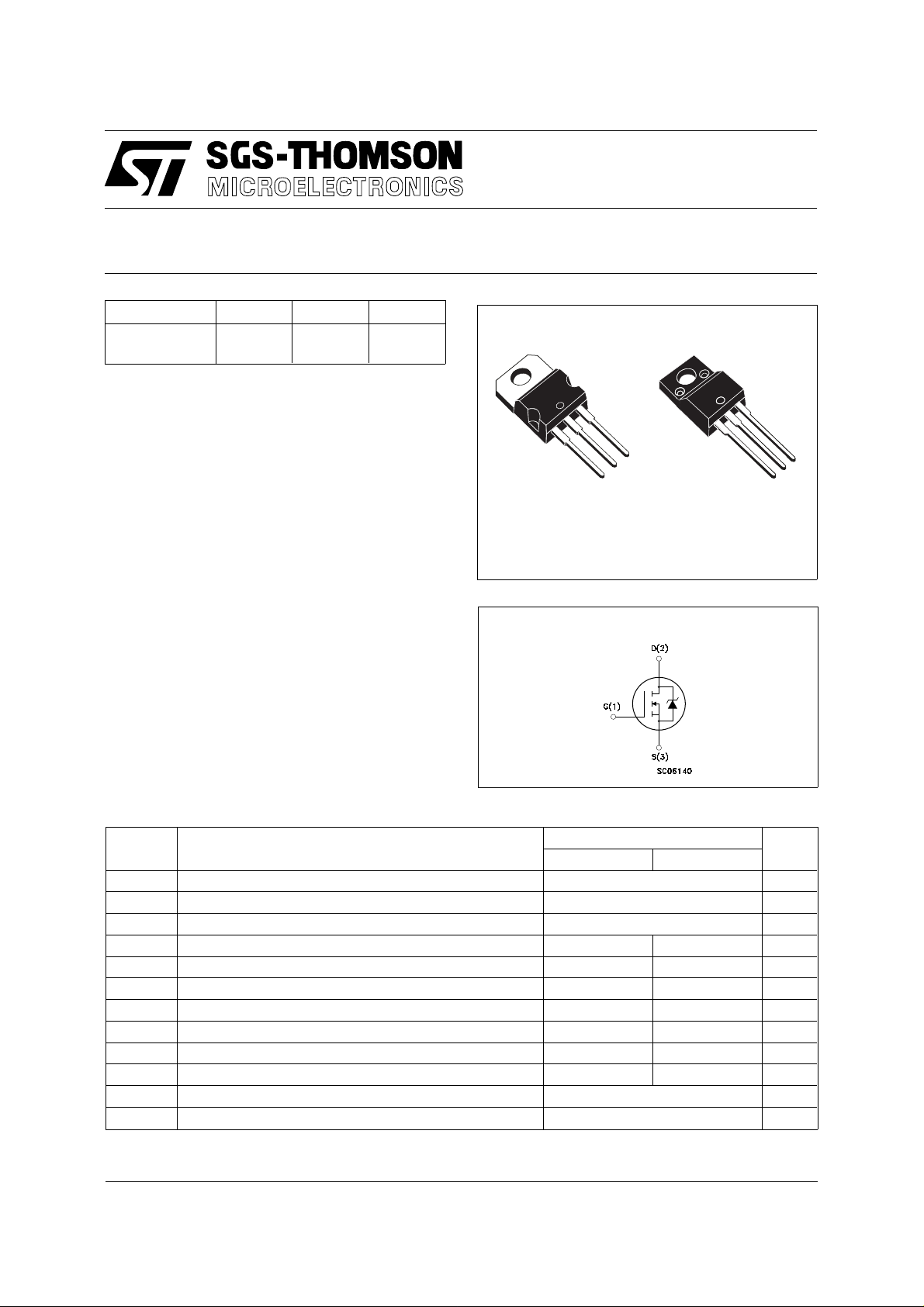
TO-220 TO-220FP
INTER NAL SCH E M ATI C DIAG RA M
3
2
1
APPLICATIONS
■ HIGH CURRENT, HIGH SPE ED SWI TCHING
■ SWITC H MODE POWER SUPPLIES (SMPS)
■ DC-AC CONVE RTERS FOR W ELDING
EQUIPMENT AND UNINTERRUPTIBLE
POWER SUPPLIES AND MOTOR DRIVE
ABSOLUTE MAXIMUM RATINGS
Symbol Parameter Value Unit
STP7NB40 STP7NB40FP
V
V
V
I
DM
P
dv/dt(
V
T
(•) Pulse width limited by safe operating area (1) ISD ≤ 7A, di/dt ≤ 200 A/µs, VDD ≤ V
This is preliminary information on a new product now in development or undergoing evaluation. Details are subject to change without notice.
January 1998
Drain-source Voltage (VGS = 0) 400 V
DS
Drain- gate Voltage (RGS = 20 kΩ)
DGR
Gate-source Voltage ± 30 V
GS
I
Drain Current (continuous) at Tc = 25 oC 7 4.4 A
D
I
Drain Current (continuous) at Tc = 100 oC 4.4 2.8 A
D
400 V
(•) Drain Current (pulsed) 28 28 A
Total Dissipation at Tc = 25 oC10035W
tot
Derating Factor 0.8 0.28 W/
1) Peak Diode Recovery voltage slope 4.5 4.5 V/ns
Insulation Withstand Voltage (DC) 2000 V
ISO
Storage Temperature -65 to 150
stg
T
Max. Operating Junction Temperature 150
j
, Tj ≤ T
(BR)DSS
JMAX
o
C
o
C
o
C
1/4

STP7NB40/FP
THERMAL DATA
TO-220 TO-220FP
R
thj-case
R
thj-amb
R
thc-sink
T
AVALANCHE CHARACTERI S TICS
Symbol Parameter Max Value Unit
I
AR
E
Thermal Resistance Junction-case Max 1.25 3.57
Thermal Resistance Junction-ambient Max
Thermal Resistance Case-sink Typ
Maximum Lead Temperature For Soldering Purpose
l
Avalanche Current, Repetitive or Not-Repetitive
(pulse width limited by T
Single Pulse Avalanche Energy
AS
(starting T
= 25 oC, ID = IAR, V
j
ma x, δ < 1%)
j
= 50 V)
DD
62.5
0.5
300
7A
300 mJ
o
C/W
o
C/W
o
C/W
o
C
ELECTRICAL CHARACTERISTICS (T
= 25 oC unless otherwise specified)
case
OFF
Symbol Parameter Test Conditions Min. Typ. Max. Unit
V
(BR)DSS
Drain-source
I
= 250 µA V
D
GS
= 0
400 V
Breakdown Voltage
I
DSS
I
GSS
Zero Gate Voltage
Drain Current (V
GS
Gate-body Leakage
Current (V
DS
= 0)
= 0)
= Max Rating
V
DS
V
= Max Rating Tc = 125 oC
DS
V
= ± 30 V
GS
1
50
± 100 nA
ON (∗)
Symbol Parameter Test Conditions Min. Typ. Max. Unit
V
GS(th)
Gate Threshold
V
= VGS ID = 250 µA
DS
345V
Voltage
R
DS(on)
Static Drain-source On
VGS = 10V ID = 3.5 A 0.75 0.9 Ω
Resistance
I
D(on)
On State Drain Current VDS > I
V
= 10 V
GS
D(on)
x R
DS(on)max
7A
DYNAMIC
Symbol Parameter Test Conditions Min. Typ. Max. Unit
gfs (∗) Forward
Transconductance
C
C
C
Input Capacitance
iss
Output Capacitance
oss
Reverse Transfer
rss
Capacitance
VDS > I
V
DS
x R
D(on)
DS(on)max
= 25 V f = 1 MHz V
ID = 3.5 A 2.5 4.2 S
= 0 705
GS
132
17
720
175
25
µA
µA
pF
pF
pF
2/4
 Loading...