

SGS Thomson Microelectronics STP6NB25, STP6NB25FP Datasheet

STP6NB25
STP6NB25FP
N-CHANNEL 250V - 0.9Ω - 6A TO-220/TO-220FP
PowerMesh MOSFET
TYPE V
STP6NB25 250 V < 1.1 Ω 6A
STP6NB25FP 250 V < 1.1 Ω 3.7 A
■ TYPICAL R
■ EXTREMELY HIGH dv/dt CAPABILITY
■ 100% AVALANCHE TESTED
■ VERY LOW INTRINSIC CAPACITANCES
■ GATE CHARGE MINIMIZED
DS
DSS
(on) = 0.9 Ω
R
DS(on)
I
D
DESCRIPTION
Using the latest high voltage MESH OVERLAY
process, STMicroelectronics has designed an advanced family of power MOSFETs with outstanding
performances. The new patent pending strip layout
coupled with theCompany’sproprieraty edge termination structure, gives the lowest R
DS(on)
per area,
exceptional avalanche and dv/dt capabilities and
unrivalled gate charge and switching characteristics.
APPLICATIONS
■ HIGH CURRENT, HIGH SPEED SWITCHING
■ UNINTERRUPTIBLE POWER SUPPLY (UPS)
■ DC-DC & DC-AC CONVERTERS FOR
TELECOM , INDUSTRIAL AND CONSUMER
ENVIRONMENT
3
2
1
TO-220
TO-220FP
INTERNAL SCHEMATIC DIAGRAM
3
2
1
ABSOLUTE MAXIMUM RATINGS
Symbol Parameter Value Unit
STP6NB25 STP6NB25FP
V
DS
V
DGR
V
GS
I
D
I
D
I
DM
P
TOT
dv/dt (1) Peak Diode Recovery voltage slope 5.5 V/ns
V
ISO
T
stg
T
(•)Pulse width limitedby safe operating area
Drain-source Voltage (VGS=0)
Drain-gate Voltage (RGS=20kΩ)
Gate- source Voltage ±30 V
Drain Current (continuos) at TC=25°C
Drain Current (continuos) at TC= 100°C
(●)
Drain Current (pulsed) 24 24 A
TotalDissipation at TC=25°C
Derating Factor 0.6 0.24 W/°C
Insulation Withstand Voltage (DC) - 2000
Storage Temperature –60 to 150 °C
Max. Operating Junction Temperature 150 °C
j
(1)ISD≤6A, di/dt ≤100A/µs, VDD≤ V
3.8 2.3 A
250 V
250 V
6 3.7 A
75 30 W
(BR)DSS,Tj≤TJMAX.
1/9Jun 2000
STP6NB25/FP
THERMAL DATA
TO-220 TO-220FP
Rthj-case Thermal Resistance Junction-case Max 1.66 4.17 °C/W
Rthj-amb Thermal Resistance Junction-ambient Max 62.5 °C/W
Rthc-sink Thermal Resistance Case-sink Typ 0.5 °C/W
T
l
AVALANCHE CHARACTERISTICS
Symbol Parameter Max Value Unit
I
AR
E
AS
ELECTRICAL CHARACTERISTICS (TCASE = 25 °C UNLESS OTHERWISE SPECIFIED)
OFF
Symbol Parameter Test Conditions Min. Typ. Max. Unit
V
(BR)DSS
I
DSS
I
GSS
Maximum Lead Temperature For Soldering Purpose 300 °C
Avalanche Current, Repetitive or Not-Repetitive
(pulse width limited by T
max)
j
Single Pulse Avalanche Energy
(starting T
Drain-source
Breakdown Voltage
Zero Gate Voltage
Drain Current (V
Gate-body Leakage
Current (V
=25°C, ID=IAR,VDD=50V)
j
I
= 250 µA, VGS=0
D
= Max Rating
V
DS
=0)
DS
GS
=0)
V
= Max Rating, TC= 125 °C
DS
= ±30V
V
GS
600 V
6A
200 mJ
1 µA
50 µA
±100 nA
ON (1)
Symbol Parameter Test Conditions Min. Typ. Max. Unit
V
GS(th)
R
DS(on)
I
D(on)
Gate Threshold Voltage
Static Drain-source On
Resistance
On State Drain Current
V
DS=VGS,ID
= 10V, ID=3 A
V
GS
V
DS>ID(on)xRDS(on)max,
= 250µA
VGS=10V
234V
0.9 1.1 Ω
6A
DYNAMIC
Symbol Parameter Test Conditions Min. Typ. Max. Unit
V
g
(1)
fs
C
iss
C
oss
C
rss
Forward Transconductance
Input Capacitance
Output Capacitance 68 pF
Reverse Transfer
Capacitance
DS>ID(on)xRDS(on)max,
ID=3A
V
= 25V, f = 1 MHz, VGS=0
DS
3S
260 pF
9pF
2/9
STP6NB25/FP
ELECTRICAL CHARACTERISTICS (CONTINUED)
SWITCHING ON
Symbol Parameter Test Conditions Min. Typ. Max. Unit
t
d(on)
t
r
Q
Q
gs
Q
gd
Turn-on Delay Time
Rise Time
TotalGate Charge
g
Gate-Source Charge 7.5 nC
Gate-Drain Charge 3 nC
SWITCHING OFF
Symbol Parameter Test Conditions Min. Typ. Max. Unit
t
r(Voff)
t
f
t
c
Off-voltage Rise Time
Fall Time 7 ns
Cross-over Time 15 ns
SOURCE DRAIN DIODE
Symbol Parameter Test Conditions Min. Typ. Max. Unit
I
SD
I
SDM
V
SD
t
rr
Q
rr
I
RRM
Note: 1. Pulsed: Pulse duration = 300 µs, duty cycle 1.5 %.
2. Pulse width limited by safe operating area.
Source-drain Current 6 A
(2)
Source-drain Current (pulsed) 24 A
(1)
Forward On Voltage
Reverse Recovery Time
Reverse Recovery Charge 720 µC
Reverse Recovery Current 9 A
V
= 125 V,ID=3A
DD
= 4.7Ω VGS=10V
R
G
(see test circuit, Figure 3)
V
= 200V, ID=6A,
DD
= 10V
V
GS
V
= 200V, ID=6A,
DD
=4.7Ω, VGS= 10V
R
G
(see test circuit, Figure 5)
ISD= 6 A, VGS=0
I
= 6 A, di/dt = 100A/µs,
SD
= 100V, Tj= 150°C
V
DD
(see test circuit, Figure 5)
9ns
9ns
12 17 nC
8ns
1.6 V
160 ns
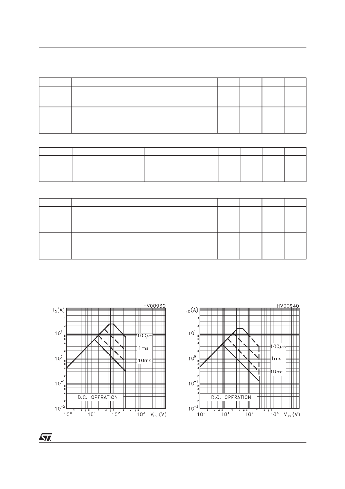
Safe Operating Area for TO-220 Safe Operating Area for TO-220FP
3/9
 Loading...