

SGS Thomson Microelectronics STP60NF06L, STB60NF06L Datasheet
STB60NF06L
STP60NF06L STP60NF06LFP
N-CHANNEL 60V - 0.012 Ω - 60A TO-220/TO-220FP/D2PAK
STripFET™ II POWER MOSFET
TYPE
STB60NF06L
STP60NF06L
STP60NF06LFP
■ TYPICAL R
■ EXCEPTIONA L dv/d t CAPABILITY
■ 100% AVALANCHE TESTED
■ APPLICATION ORIENTED
V
DSS
60 V
60 V
60 V
(on) = 0.012Ω
DS
R
DS(on)
<0.014
<0.014
<0.014
I
D
60 A
Ω
60 A
Ω
60 A(*)
Ω
CHARACTERIZATION
■ 175
■ LOW THRESHOLD DRIVE
■ SURFACE-MOUNTING D
o
C OPERATING RANGE
2
PAK (TO-263)
POWER PACKAGE IN TAPE & REEL
(SUFFIX “T4”)
DESCRIPTION
This MOSFET series realized with STMicroelectronics
unique STripFET process has specifically been designed
to minimize input capacitance and gate charge. It is
therefore suitable as primary switch in advanced highefficiency, high-frequency isolate d DC-DC c onverters for
Telecom and Computer a pplications. It is also intended
for any applications with low gate drive requirements.
APPLICATIONS
■ HIGH-EFFICIENCY DC-DC CONVERTERS
■ AUTOMOTIVE
3
2
1
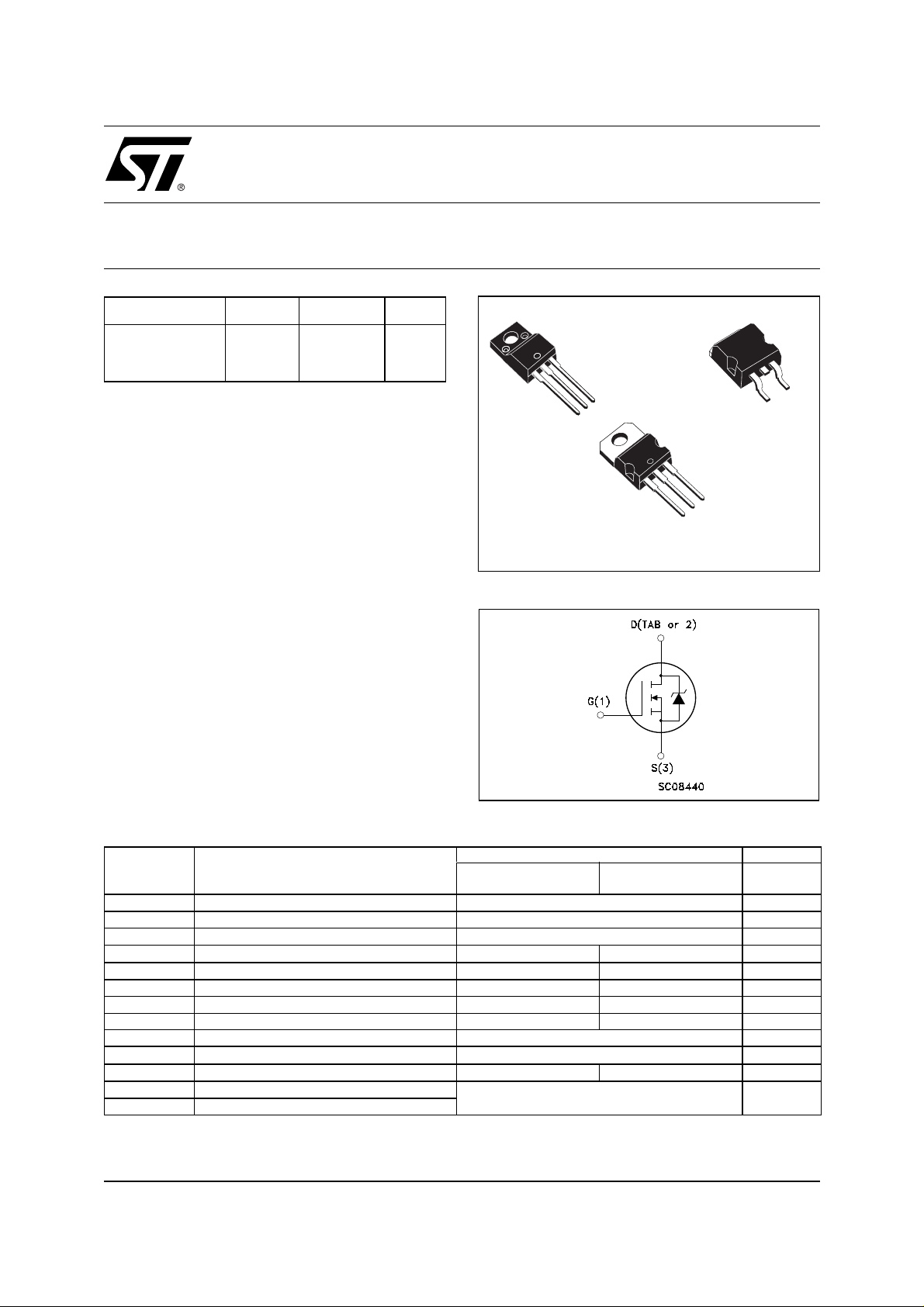
TO-220FP
3
2
1
TO-220
INTERNAL SCHEMATIC DIAGRAM
1
D2PAK
TO-263
(Suffix “T4”)
3
ABSOLUTE MAXIMUM RATINGS
Symbol Parameter Value Unit
Drain-source Voltage (VGS = 0)
Drain-gate Voltage (RGS = 20 kΩ)
Gate- source Voltage ± 15 V
Drain Current (continuous) at TC = 25°C
Drain Current (continuous) at TC = 100°C
•)
Drain Current (pulsed) 240 240(*) A
Total Dissipation at TC = 25°C
V
I
V
V
DM
P
DS
DGR
GS
I
D
I
D
(
tot
Derating Factor 0.73 0.2 W/°C
(1)
dv/dt
E
AS
V
ISO
T
stg
T
j
(
Pulse widt h l i m i ted by safe o perating area.
•)
(*) Ref er to S OA for the max allowable current values on FP-typ e
due to Rth value
.
Peak Diode Recovery voltage slope 20 V/ns
(2)
Single Pulse Avalanche Energy 320 mJ
Insulation Withstand Voltage (DC) ------ 2000 V
Storage Temperature
Operating Junction Temperature
STB60NF06 L
STP60NF06 L
60 60(*) A
42 42(*) A
110 30 W
-55 to 175 °C
≤ 60A, di/dt ≤ 600A/µs , VDD ≤ 48V, Tj ≤ T
(1) I
SD
(2) Starting Tj = 25 oC, ID = 30A, VDD = 30V
STP60NF06LF P
60 V
60 V
JMAX.
1/11July 2003
STB60NF06L STP60NF06L/FP
THERMA L D ATA
D2PAK
TO-220
Rthj-case Thermal Resistance Junction-case Max 1.36 5.0 °C/W
TO-220FP
Rthj-amb
Rthj-pcb
T
(#)Only for SMD,
ELECTRICAL CHARACTERISTICS (T
Thermal Resistance Junction-ambient
Thermal Resistance Junction-pcb
Maximum Lead Temperature For Soldering Purpose
l
When Mounted on 1 inch2 FR-4 board, 2 oz of Cu.
(#)
= 25 °C unless otherwise specified)
case
Max
Max
62.5
35
300
OFF
Symbol Parameter Test Conditions Min. Typ. Max. Unit
I
Drain-source
Breakdown Voltage
Zero Gate Voltage
Drain Current (V
GS
Gate-body Leakage
Current (V
DS
= 0)
= 0)
ON
V
(BR)DSS
I
DSS
I
GSS
(1)
Symbol Parameter Test Conditions Min. Typ. Max. Unit
V
GS(th)
R
DS(on)
Gate Threshold Voltage
Static Drain-source On
Resistance
= 250 µA, VGS = 0
D
V
= Max Rating
DS
V
= Max Rating TC = 125°C
DS
V
= ± 15V
GS
V
= VGS I
DS
= 5 V ID = 30 A
V
GS
V
= 10 V ID = 30 A
GS
= 250 µA
D
60 V
1
10
±100 nA
1V
0.014
0.012
0.016
0.014
°C/W
°C/W
°C
µA
µA
Ω
Ω
DYNAMIC
Symbol Parameter Test Conditions Min. Typ. Max. Unit
(*)
g
fs
C
iss
C
oss
C
rss
Forward Transconductance
Input Capacitance
Output Capacitance
Reverse Transfer
Capacitance
V
= 15 V ID=30 A
DS
= 25V, f = 1 MHz, VGS = 0
V
DS
20 S
2000
360
125
pF
pF
pF
2/11
STB60NF06L STP60NF 06L/FP
ELECTRICAL CHARACTERISTICS (continued)
SWITCHING ON
Symbol Parameter Test Conditions Min. Typ. Max. Unit
= 30 V ID = 30 A
t
d(on)
Turn-on Delay Time
t
r
Rise Time
V
DD
R
= 4.7 Ω VGS = 4.5 V
G
(Resistive Load, Figure 3)
Q
Q
gs
Q
gd
Total Gate Charge
g
Gate-Source Charge
Gate-Drain Charge
= 48 V ID= 60 A VGS= 4.5V
V
DD
SWITCHING OFF
Symbol Parameter Test Conditions Min. Typ. Max. Unit
= 30V ID = 30 A
t
d(off)
Turn-off Delay Time
t
f
Fall Time
V
DD
R
= 4.7Ω, V
G
GS
= 4.5 V
(Resistive Load, Figure 3)
SOURCE DRAIN DIODE
Symbol Parameter Test Conditions Min. Typ. Max. Unit
I
SD
I
SDM
V
SD
t
rr
Q
rr
I
RRM
(*)
Pulsed: P ul se duration = 300 µs, duty cycle 1.5 %.
(•)
Pulse width l i m i ted by safe operating area.
Source-drain Current
(•)
Source-drain Current (pulsed)
(*)
Forward On Voltage
Reverse Recovery Time
Reverse Recovery Charge
Reverse Recovery Current
I
= 60A VGS = 0
SD
= 60 A di/dt = 100A/µs
I
SD
V
= 30 V Tj = 150°C
DD
(see test circuit, Figure 5)
35
220
35
10
20
55
30
60
240
1.3 V
110
250
4.5
ns
ns
nC
nC
nC
ns
ns
A
A
ns
nC
A
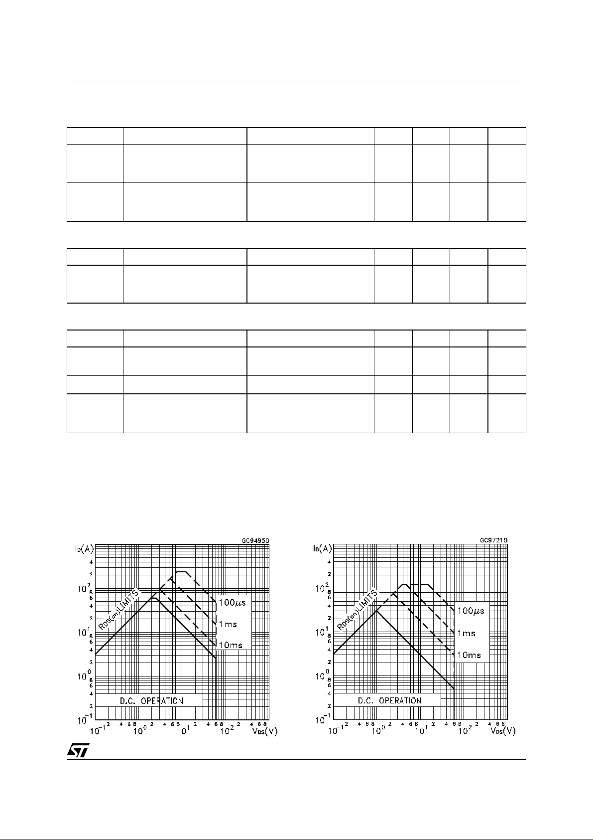
Safe Operating Area Safe Operating Area for TO-220FP
3/11
STB60NF06L STP60NF06L/FP
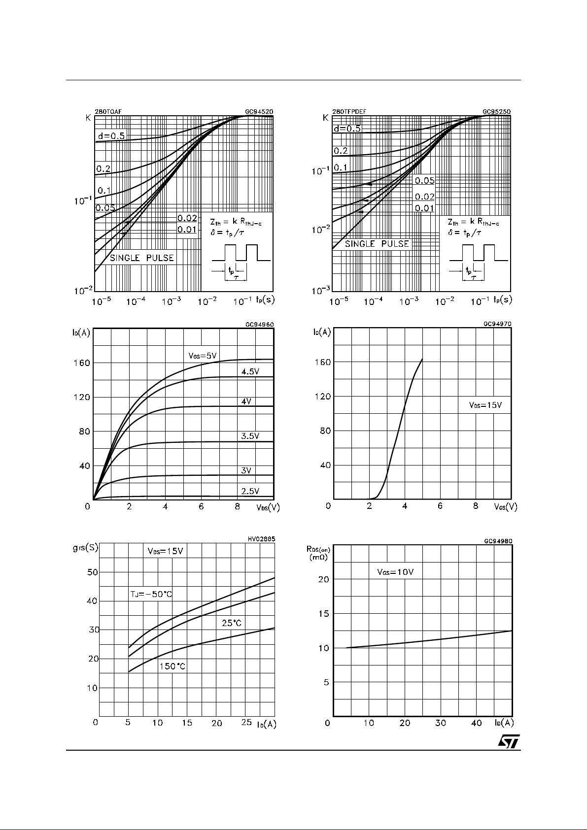
Thermal Impedance Thermal Impedance for TO-220FP
Output Characteristics Transfer Characteristics
Transconductance Static Drain-source On Resistance
4/11
 Loading...