

SGS Thomson Microelectronics STP60NF03L Datasheet
STP60NF03L
N-CHANNEL 30V - 0.008
TYPE V
ST P60NF03L 30 V < 0. 010 Ω 60 A
■ TYPICALR
■ LOW THRESHOLDDRIVE
DS(on)
DSS
= 0.008 Ω
DESCRIPTION
This Power Mosfet is the latest development of
STMicroelectronics unique ”Single Feature
Size” strip-based process. The resulting
transistor shows extremely high packing density
for low on-resistance, rugged avalance
characteristics and less critical alignment steps
therefore a remarkable manufacturing
reproducibility.
APPLICATIONS
■ HIGHCURRENT, HIGH SPEEDSWITCHING
■ MOTORCONTROL, AUDIOAMPLIFIERS
■ DC-DC& DC-AC CONVERTERS
■ AUTOMOTIVEENVIRONMENT(INJECTION,
ABS, AIR-BAG, LAMPDRIVERS,Etc. )
R
DS(on)
I
D
Ω
- 60A TO-220
STripFET POWER MOSFET
PRELIMINARY DATA
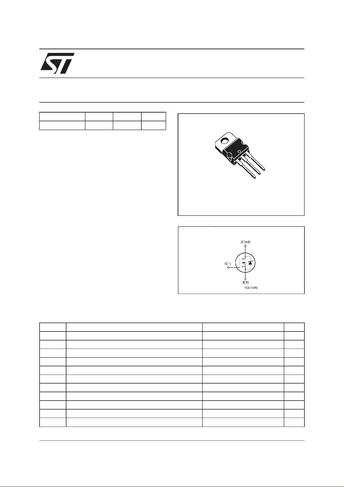
3
2
1
TO-220
INTERNAL SCHEMATIC DIAGRAM
ABSOLUTE MAXIMUM RATINGS
Symbol Parameter Value Unit
V
V
V
I
DM
P
E
AS(1
T
(•) Pulse width limited by safe operating area (1) starting Tj
September 1999
Dra in- sour c e Volt age ( VGS=0) 30 V
DS
Dra in- gate V ol t age (RGS=20kΩ)30V
DGR
Gat e-source Voltage
GS
I
Dra in Current ( continuous) at Tc=25oC60A
D
I
Dra in Current ( continuous) at Tc=100oC42A
D
(•) D rain Current (pulsed) 240 A
Tot al Dissipat ion at Tc=25oC 100 W
tot
Der ati ng Fac t or 0.67 W/
) Single Pulse Avalanche Energy 650 mJ
St orage Temper at ure -65 t o 175
stg
T
Max. O perating Junc t ion T emperatur e 175
j
=25oC,ID=30A,VDD= 20V
20 V
±
o
C
o
C
o
C
1/6
STP60NF03L
THERMAL DATA
R
thj-case
Rthj-amb
R
thc-sink
T
Ther mal Resistanc e Junct ion-case Max
Ther mal Resistanc e Junct ion-ambient Max
Ther mal Resistanc e Case-sink Ty p
Maximum Lead Temperature For Soldering Purpos e
l
1.5
62.5
0.5
300
o
C/W
oC/W
o
C/W
o
C
ELECTRICAL CHARACTERISTICS
=25oC unless otherwisespecified)
(T
case
OFF
Symbol Parameter Test Conditions Min. Typ. Max. Unit
V
(BR)DSS
Drain-source
ID=250µAVGS=0 30 V
Break dow n V o lt age
I
DSS
I
GSS
Zero Gate Voltage
Drain Curr e nt (V
GS
Gat e- bod y Leak ag e
Current (V
DS
=0)
=0)
V
=MaxRating
DS
=MaxRating Tc=125oC
V
DS
V
= ± 20 V ± 100 nA
GS
1
10
ON(∗)
Symbol Parameter Test Conditions Min. Typ. Max. Unit
V
GS(th)
R
DS(on)
I
D(on)
Gate Threshold Voltage VDS=VGSID= 250 µA11.52.5V
Sta t ic Drain-s ource On
Resistance
VGS=10V ID=30A
=4.5V ID=30A
V
GS
On State Drain Current VDS>I
D(on)xRDS(on)max
0.008
0.0095
60 A
0.010
0.015ΩΩ
VGS=10V
DYNAMIC
Symbol Parameter Test Conditions Min. Typ. Max. Unit
g
(∗)Forward
fs
Tr ansc on duc tance
C
C
C
Input Capacitance
iss
Out put Capac it ance
oss
Reverse Tr ansfer
rss
Capacit a nc e
VDS>I
D(on)xRDS(on)maxID
=30 A 60 S
VDS=25V f=1MHz VGS= 0 2550
630
215
µ
µA
pF
pF
pF
A
2/6
 Loading...