

SGS Thomson Microelectronics STP60NE10FP, STP60NE10 Datasheet
STP60NE10
STP60NE10FP
N - CHANNEL 100V - 0.016Ω - 60A TO-220/TO-220FP
STripFET POWER MOSFET
TYPE V
ST P60NE10
ST P60NE10FP
■ TYPICALR
■ EXCEPTIONALdv/dt CAPABILITY
■ 100%AVALANCHETESTED
■ APPLICATIONORIENTED
DS(on)
DSS
100 V
100 V
= 0.016 Ω
CHARACTERIZATION
DESCRIPTION
This PowerMOSFET is the latest developmentof
STMicroelectronics unique ”Single Feature
Size” strip-based process.The resulting transi-
stor showsextremelyhigh packing densityfor low
on-resistance, rugged avalanche characteristics
and less critical alignment steps therefore a remarkablemanufacturingreproducibility.
APPLICATIONS
■ SOLENOIDAND RELAYDRIVERS
■ MOTORCONTROL, AUDIOAMPLIFIERS
■ DC-DCCONVERTERS
■ AUTOMOTIVEENVIRONMENT(INJECTION,
ABS, AIR-BAG, LAMPDRIVERS,Etc.)
R
DS(on)
<0.022Ω
<0.022Ω
I
D
60 A
30 A
3
2
1
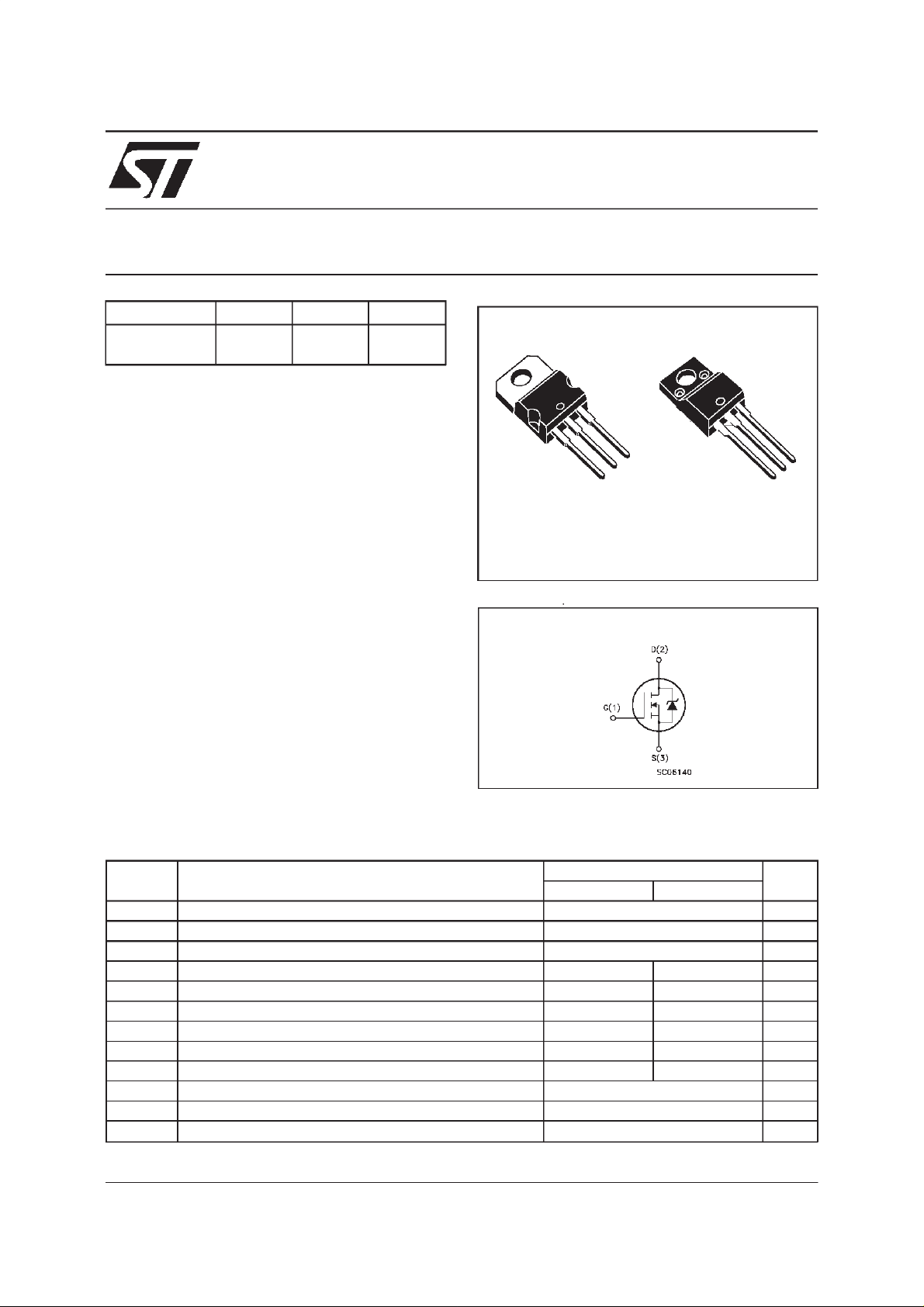
TO-220 TO-220FP
INTERNAL SCHEMATIC DIAGRAM
3
2
1
ABSOLUTE MAXIMUM RATINGS
Symbol Parameter Value Unit
ST P60NE10 ST P60NE10FP
V
V
V
I
DM
P
V
dv/ dt Peak Diode Recovery v olt a ge slope 7 V/ns
T
(•) Pulsewidth limited by safeoperating area (1)ISD≤ 60 A, di/dt ≤ 300 A/µs, VDD≤ V
May 1999
Drain-source Voltage (VGS= 0) 100 V
DS
Drain- gate Voltage (RGS=20kΩ) 100 V
DGR
Gate-source Voltage ± 20 V
GS
I
Drain Curre nt (cont inuous) at Tc=25oC6030A
D
Drain Curre nt (cont inuous) at Tc=100oC4221A
I
D
(•) Dr ain Curre nt (pulse d) 240 120 A
Total Dissipation at Tc=25oC 160 50 W
tot
Derat ing F ac tor 1.06 0.37 W/
Ins ulat ion W ithstand Voltage (DC) 20 00 V
ISO
Sto rage Temperat ure -65 t o 175
stg
T
Max. Oper ating Junction Tempe rat ure 175
j
(BR)DSS,Tj≤TJMAX
o
C
o
C
o
C
1/9
STP60NE10/FP
THERMAL DATA
TO-220 TO-220FP
R
thj-case
R
thj-amb
R
thc-sink
T
AVALANCHE CHARACTERISTICS
Symbol Parameter Max V alue Unit
I
AR
E
Ther mal Resistanc e Junct ion-case Max 0.94 2.7
Ther mal Resistanc e Junct ion-ambient Max
Ther mal Resistanc e Case-sink Ty p
Maximum L ead Temperature F or Solder ing Purpose
l
Avalanche Current, Repetitive or Not-Repetitive
(pulse width limited by T
Single Pul se Avalanche E nergy
AS
(starting T
=25oC, ID=IAR,VDD=35V)
j
max)
j
62.5
0.5
300
60 A
100 mJ
o
C/W
o
C/W
o
C/W
o
C
ELECTRICAL CHARACTERISTICS
=25oC unless otherwisespecified)
(T
case
OFF
Symbol Parameter Test Conditions Min. Typ. Max. Unit
V
(BR)DSS
Drain-source
ID=250µAVGS= 0 100 V
Break dow n Vo lt age
I
DSS
I
GSS
Zero Gate Voltage
Drain Curre nt (V
GS
Gat e- bod y Leakage
Current (V
DS
=0)
=0)
V
=MaxRating
DS
=MaxRating Tc= 125oC
V
DS
V
=± 20 V
GS
1
10
100 nA
±
ON (∗)
Symbol Parameter Test Conditions Min. Typ. Max. Unit
V
GS(th)
R
DS(on)
Gate Threshold Voltage VDS=VGSID= 250µA 234V
Sta t ic Drain-s ource O n
VGS=10V ID= 30 A 0.016 0.022
Resistance
I
D(on)
On StateDrain Current VDS>I
D(on)xRDS(on )max
60 A
VGS=10V
DYNAMIC
Symbol Parameter Test Conditions Min. Typ. Max. Unit
g
(∗)Forward
fs
Tr ansc on duc tance
C
C
C
Input Capaci t ance
iss
Out put Capac it ance
oss
Reverse Transfer
rss
Capacit a nc e
VDS>I
D(on)xRDS(on )maxID
=18 A 30 S
VDS=25V f=1MHz VGS= 0 5300
640
215
µA
µA
Ω
pF
pF
pF
2/9
STP60NE10/FP
ELECTRICAL CHARACTERISTICS
(continued)
SWITCHINGON
Symbol Parameter Test Conditions Min. Typ. Max. Unit
t
d(on)
t
Tur n-on Delay Time
Rise Time
r
VDD=50V ID=30A
R
=4.7
G
Ω
VGS=10V
28
100
(Resis t iv e Load, s ee f ig. 3 )
Q
Q
Q
Tot al Gate Charge
g
Gat e- Source Char g e
gs
Gate-Drain Charge
gd
VDD=80V ID=60A VGS= 10 V 142
27
59
185 nC
SWITCHINGOFF
Symbol Parameter Test Conditions Min. Typ. Max. Unit
t
d(off)
Tur n-of f Dela y T ime
t
Fall T ime
f
VDD=50V ID=30A
=4.7 Ω VGS=10V
R
G
160
45
(Resis t iv e Load, s ee f ig. 3 )
t
r(Voff)
t
t
Off-volt age Rise Time
Fall T ime
f
Cross-over Tim e
c
V
=80V ID=60A
clamp
=4.7 Ω VGS=10V
R
G
(Indu ctive Load , see fig . 5)
40
45
85
SOURCE DRAIN DIODE
Symbol Parameter Test Conditions Min. Typ. Max. Unit
I
SD
I
SDM
V
SD
t
Q
I
RRM
(∗) Pulsed: Pulse duration = 300µs, duty cycle 1.5 %
(•) Pulse width limited by safe operating area
Sou rc e-d rai n Cu rre nt
(•)
Sou rc e-d rai n Cu rre nt
60
240
(pulsed)
(∗)ForwardOnVoltage ISD=60A VGS=0 1.5 V
Reverse Recovery
rr
Time
Reverse Recovery
rr
ISD= 60 A di /dt = 100 A/µs
=50V Tj=150oC
V
DD
(s ee t est c ircu it , f ig. 5)
170
1.02
Charge
Reverse Recovery
12
Current
ns
ns
nC
nC
ns
ns
ns
ns
ns
A
A
ns
µC
A
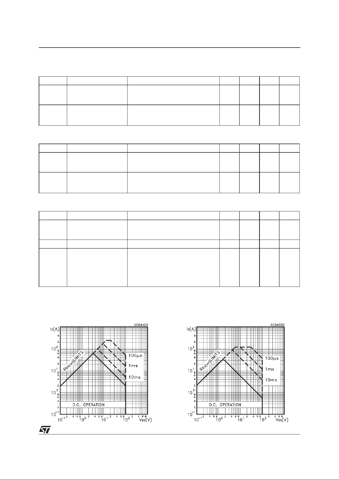
Safe Operating Areafor TO-220 Safe Operating Areafor TO-220FP
3/9
 Loading...