

SGS Thomson Microelectronics STP60NE06L-16FP, STP60NE06L-16 Datasheet
STP60NE06L-16
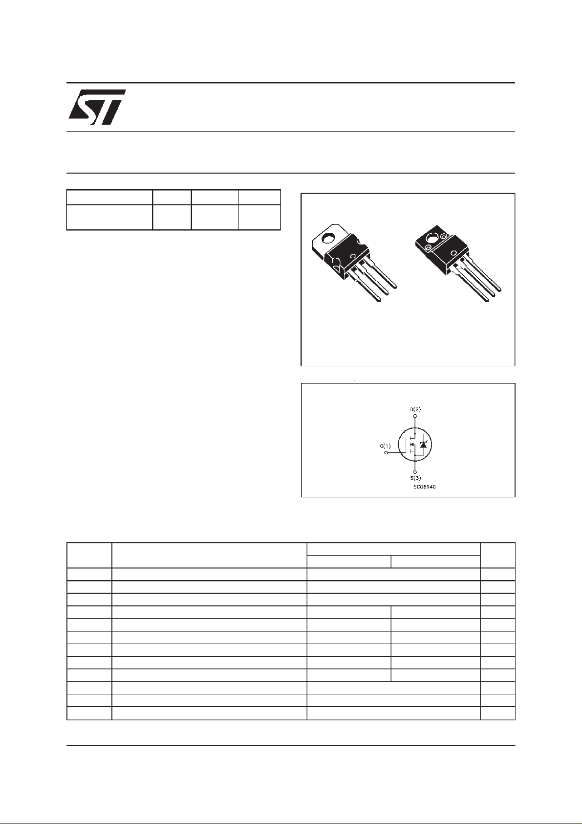
N - CHANNEL 60V - 0.014Ω - 60A TO-220/TO-220FP
TYPE V
ST P60NE06L-16
ST P60NE06L-16F P
■ TYPICALR
■ AVALANCHERUGGEDTECHNOLOGY
■ LOW GATE CHARGE
■ HIGHCURRENT CAPABILITY
■ 175
■ LOW THRESHOLDDRIVE
o
DS(on)
C OPERATINGTEMPERATURE
DSS
60 V
60 V
= 0.014 Ω
DESCRIPTION
This Power Mosfet is the latest development of
STMicroelectronisunique ”Single Feature Size”
strip-based process. The resulting transistor
shows extremely high packing density for low onresistance, rugged avalanche characteristicsand
less critical alignment steps therefore a remarkable manufacturingreproducibility.
R
DS(on)
<0.016Ω
<0.016Ω
I
D
60 A
35 A
STP60NE06L-16FP
STripFET POWER MOSFET
3
2
1
TO-220 TO-220FP
INTERNAL SCHEMATIC DIAGRAM
3
2
1
APPLICATIONS
■ HIGHCURRENT, HIGH SPEED SWITCHING
■ SOLENOIDAND RELAYDRIVERS
■ DC-DC& DC-ACCONVERTERS
■ AUTOMOTIVEENVIRONMENT
ABSOLUTE MAXIMUM RATINGS
Symbol Parameter Value Unit
STP 60NE06L- 16 STP 60NE 0 6L - 16 F P
V
V
V
I
DM
P
V
dv/ dt Peak Diode Recovery voltage slope 6 V/ ns
T
(•) Pulsewidth limited by safeoperating area (1)ISD≤ 60 A, di/dt ≤ 300 A/µs, VDD≤ V
May 2000
Drain-source Voltage (VGS=0) 60 V
DS
Drain- gate Voltage (RGS=20kΩ)60V
DGR
Gate-source Voltage ± 15 V
GS
I
Drain Curre nt (cont i nuous) at Tc=25oC60 35A
D
Drain Curre nt (cont i nuous) at Tc=100oC42 24A
I
D
(•) Drain Curre nt (pulse d) 240 140 A
Total Dissipation at Tc=25oC15045W
tot
Derat ing F ac tor 1 0.3 W/
Ins ulat ion W i th s t and Voltage (DC) 2 000 V
ISO
Sto rage Temperat ure -65 to 175
stg
T
Max. Operat ing Junction Tempera t ure 175
j
(BR)DSS,Tj≤TJMAX
o
C
o
C
o
C
1/9
STP60NE06L-16/FP
THERMAL DATA
TO-220 TO-220FP
R
thj-case
R
thj-amb
R
thc-sink
T
AVALANCHE CHARACTERISTICS
Symbol Parameter Max V alue Unit
I
AR
E
Ther mal Resistanc e Junct ion-case Max 0.94 2.7
Ther mal Resistanc e Junct ion-ambient Max
Ther mal Resistanc e Case-sink Ty p
Maximum L ead Temperature F or Solder ing P urp os e
l
Avalanche Current, R epetitive or Not-Repetitive
(pulse width limited by T
Single Pul se Avalanche Ener gy
AS
(starting T
=25oC, ID=IAR,VDD=25V)
j
max)
j
62.5
0.5
300
60 A
400 mJ
o
C/W
o
C/W
o
C/W
o
C
ELECTRICAL CHARACTERISTICS
=25oC unless otherwisespecified)
(T
case
OFF
Symbol Parameter Test Conditions Min. Typ. Max. Unit
V
(BR)DSS
Drain-source
ID=250µAVGS=0 60 V
Break dow n Vo lt age
I
DSS
I
GSS
Zero Gate Voltage
Drain Curre nt (V
GS
Gat e- bod y Leakag e
Current (V
DS
=0)
=0)
V
=MaxRating
DS
=MaxRating Tc= 125oC
V
DS
V
=± 15 V
GS
1
10
100 nA
±
ON (∗)
Symbol Parameter Test Conditions Min. Typ. Max. Unit
V
GS(th)
R
DS(on)
I
D(on)
Gate Threshold Volt age VDS=VGSID= 250µA11.62.5V
Sta t ic Drain-s our c e On
Resistance
VGS=5V ID=30A
=10V ID=30A
V
GS
On State Drain Current VDS>I
D(on)xRDS(on )max
0.014
0.012
60 A
0.016
0.014ΩΩ
VGS=10V
DYNAMIC
Symbol Parameter Test Conditions Min. Typ. Max. Unit
g
(∗)Forward
fs
Tr ansc on duc tance
C
C
C
Input Capaci t ance
iss
Out put Capac itance
oss
Reverse Transfer
rss
Capacit a nc e
VDS>I
D(on)xRDS(on )maxID
=30 A 30 S
VDS=25V f=1MHz VGS= 0 4150
590
150
µA
µA
pF
pF
pF
2/9
STP60NE06L-16/FP
ELECTRICAL CHARACTERISTICS
(continued)
SWITCHING ON
Symbol Parameter Test Conditions Min. Typ. Max. Unit
t
d(on)
t
Tur n-on Delay Time
Rise Time
r
VDD=30V ID=30A
R
=4.7
G
Ω
VGS=5V
50
155
(Resis t iv e Load, see fig. 3)
Q
Q
Q
Tot al Gate Charge
g
Gat e- Source Charge
gs
Gate-Drain Charge
gd
VDD=40V ID=60A VGS=5V 55
15
30
70 nC
SWITCHING OFF
Symbol Parameter Test Conditions Min. Typ. Max. Unit
t
d(off)
Tur n-of f Dela y Tim e
t
Fall T ime
f
VDD=30V ID=30A
R
G
=4.7
Ω
VGS=5V
125
25
(Resis t iv e Load, see fig. 3)
t
r(Voff)
t
t
Off-volt age Rise Time
Fall T ime
f
Cross-over Tim e
c
VDD=48V ID=20A
R
=4.7
G
Ω
VGS=5V
(Indu ct iv e Load, see fig . 5)
45
220
280
SOURCEDRAINDIODE
Symbol Parameter Test Conditions Min. Typ. Max. Unit
I
SD
I
SDM
V
SD
t
Q
I
RRM
(∗) Pulsed:Pulse duration = 300µs, duty cycle 1.5%
(•) Pulse width limited by safeoperating area
Source-drain Current
(•)
Source-drain Current
60
240
(pulsed)
(∗)ForwardOnVoltage ISD=60A VGS=0 1.5 V
Reverse Recovery
rr
Time
Reverse Recovery
rr
ISD= 60 A di/dt = 100 A/µs
=30V TJ=150oC
V
DD
(see test circuit, fig. 5)
85
300
Charge
Reverse Recovery
7
Current
ns
ns
nC
nC
ns
ns
ns
ns
ns
A
A
ns
µ
A
C
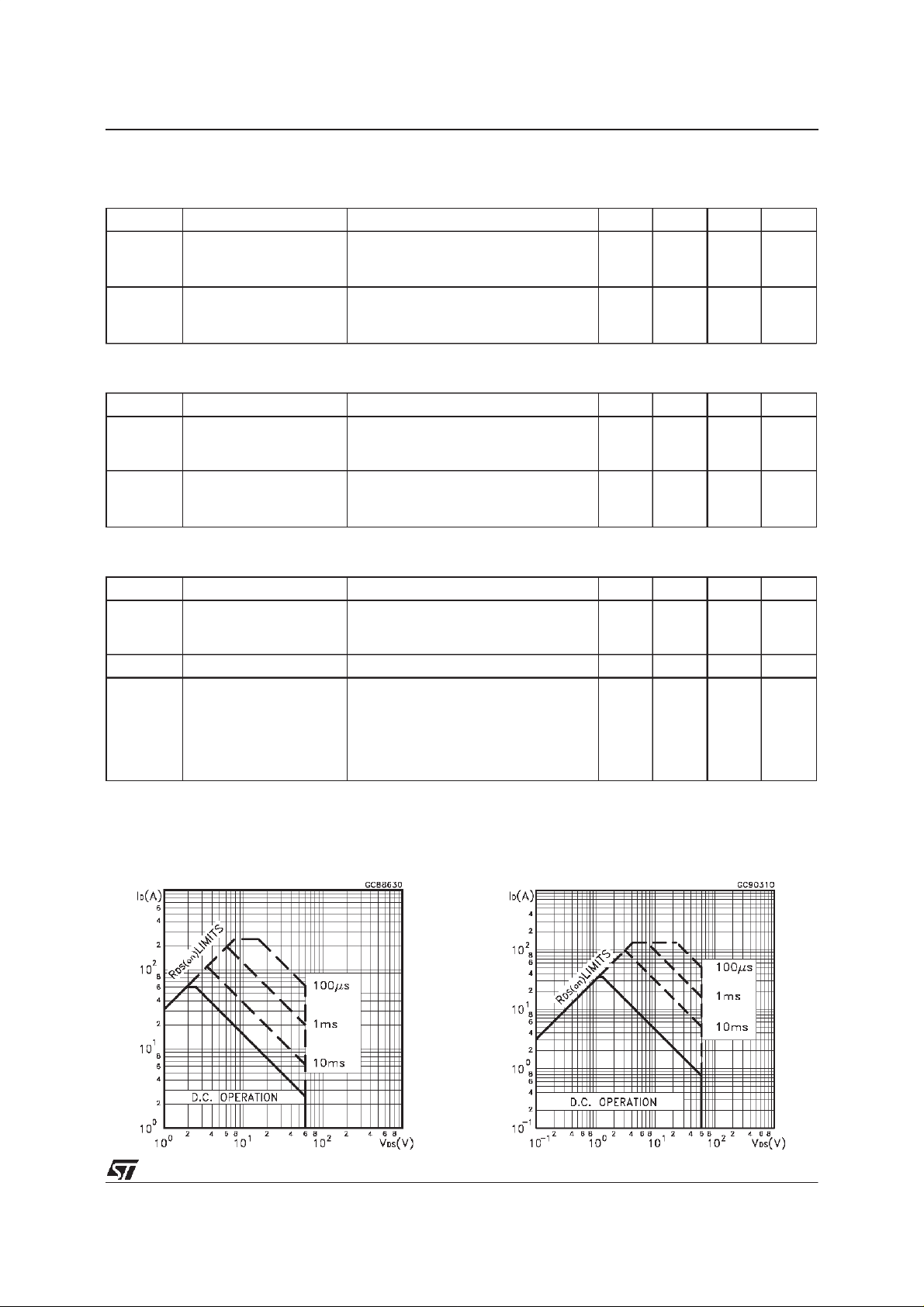
SafeOperating Area for TO-220 SafeOperating Area for TO-220FP
3/9
 Loading...