

SGS Thomson Microelectronics STP60NE06-16FP, STP60NE06-16 Datasheet
STP60NE06-16
STP60NE06-16FP
N - CHANNEL ENHANCEMENT MODE
” SINGLEFEATURE SIZE ” POWER MOSFET
TYPE V
STP 60NE06-16
STP 60NE06-16F P
■ TYPICALR
■ EXCEPTIONALdV/dt CAPABILTY
■ 100% AVALANCHETESTED
■ LOW GATE CHARGE 100
■ HIGH dV/dt CAPABILITY
■ APPLICATIONORIENTED
DS(on)
DSS
60 V
60 V
=0.013 Ω
R
DS(on)
<0.016Ω
<0.016Ω
o
C
I
D
60 A
35 A
CHARACTERIZATION
DESCRIPTION
This Power Mosfet is the latest development of
SGS-THOMSON unique ”Single Feature Size”
process whereby a single body is implanted on a
strip layout structure. The resulting transistor
shows extremely high packing density for low onresistance, rugged avalanche characteristics and
less critical alignment steps therefore a remarkable manufacturingreproducibility.
APPLICATIONS
■ DC MOTOR CONTROL
■ DC-DC& DC-AC CONVERTERS
■ SYNCHRONOUS RECTIFICATION
3
2
1
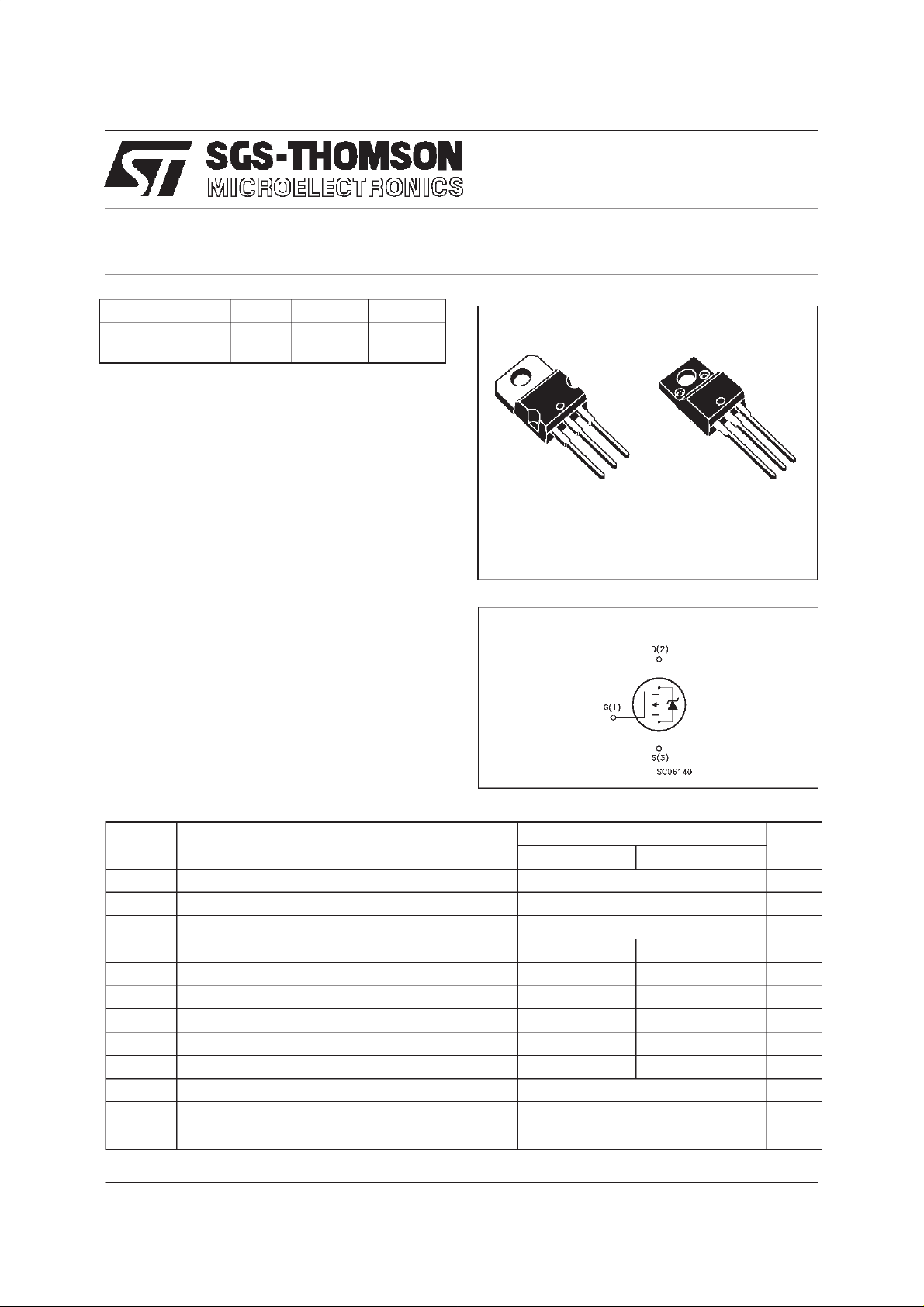
TO-220 TO220FP
INTERNAL SCHEMATIC DIAGRAM
3
2
1
ABSOLUTE MAXIMUM RATINGS
Symbol Parameter Value Unit
STP60NE06-16 STP60NE06-16FP
V
V
V
I
DM
P
V
dV/ dt Peak Diod e Rec ov ery voltage slop e 6 V/ns
T
(•) Pulse width limitedby safe operating area (1)ISD≤ 60 A,di/dt ≤ 300 A/µs, VDD≤ V
December 1997
Drain-s ource Voltage (VGS=0) 60 V
DS
Drain- gate Voltage (RGS=20kΩ)
DGR
Gate-source Voltage ± 20 V
GS
I
Drain Current (co nt inu ous) at Tc=25oC6035A
D
I
Drain Current (co nt inu ous) at Tc=100oC4224A
D
60 V
(•) Drain Current (puls ed) 240 240 A
Tot al D i ss ipa t ion at Tc=25oC 150 40 W
tot
Derat ing Fact or 1 0.3 W/
Insulation W ithstand Voltage (DC) 2000 V
ISO
Sto rage Temper at ure -65 t o 175
stg
T
Max. O per ating J unc t i on Temper at u re 175
j
(BR)DSS,Tj≤TJMAX
o
C
o
C
o
C
1/9
STP60NE06-16/FP
THERMAL DATA
TO - 2 20 TO - 220FP
R
thj-case
R
thj-amb
R
thc-sin k
T
AVALANCHE CHARACTERISTICS
Symb o l Parameter Max Value Uni t
I
AR
E
Ther mal Resistance Ju nc t io n- case Max 1 3.75
Ther mal Resistance Ju nc t io n- ambient Max
Ther mal Resistance Ca s e-sink Typ
Maximum Lead Tem p er at u r e Fo r Soldering Purpose
l
Avalanche Curr ent, Repetit iv e or Not-Repetit ive
(pulse width limi t ed by T
Single Pulse Aval anche Energ y
AS
(starti ng T
=25oC, ID=IAR,VDD=25V)
j
max, δ <1%)
j
62.5
0.5
300
60 A
350 mJ
o
C/W
o
C/W
o
C/W
o
C
ELECTRICAL CHARACTERISTICS (T
=25oC unlessotherwisespecified)
case
OFF
Symbol Paramet er Test Cond itions Min. Typ . Max. Unit
V
(BR)DSS
Drain-source
= 250 µAVGS=0
I
D
60 V
Break dow n Voltage
I
DSS
I
GSS
Zero Gate Voltage
Drain Current (V
GS
Gat e- bod y Le akage
Current (V
DS
=0)
=0)
=MaxRating
V
DS
V
=MaxRating Tc=125oC
DS
= ± 20 V
V
GS
1
10
± 100 nA
ON (∗)
Symbol Paramet er Test Cond itions Min. Typ . Max. Unit
V
GS(th )
R
DS(on)
Gat e Thr e shold Voltage
St at ic D rain-source O n
V
DS=VGSID
=250µA
VGS= 10V ID=30A 0.013 0.016 Ω
234V
Resistance
I
D(on)
On State Drain Curr ent VDS>I
D(on)xRDS(on)max
60 A
VGS=10V
DYNAMIC
Symbol Paramet er Test Cond itions Min. Typ . Max. Unit
g
(∗)Forward
fs
Tr ansc on ductance
C
C
C
Input Capacitanc e
iss
Out put Ca pac itance
oss
Reverse Tr ansfer
rss
Capacit a nc e
VDS>I
D(on)xRDS(on)maxID
=30 A 20 35 S
VDS=25V f=1MHz VGS= 0 4600
580
140
6200
800
200
µA
µA
pF
pF
pF
2/9
STP60NE06-16/FP
ELECTRICAL CHARACTERISTICS (continued)
SWITCHINGON
Symbol Paramet er Test Cond itions Min. Typ . Max. Unit
t
d(on)
t
Q
Q
Q
SWITCHINGOFF
Symbol Paramet er Test Cond itions Min. Typ . Max. Unit
t
r(Voff)
t
SOURCE DRAIN DIODE
Symbol Paramet er Test Cond itions Min. Typ . Max. Unit
I
SD
I
SDM
V
SD
t
Q
I
RRM
(∗) Pulsed: Pulse duration =300 µs, duty cycle 1.5 %
(•) Pulse width limited by safe operating area
Turn-on Time
Rise T ime
r
Tot al Gate Char ge
g
Gate-Source Charge
gs
Gat e- Drain Charge
gd
Off -voltage R ise Time
t
Fall T ime
f
Cross-over Time
c
Source-drain Current
(•)
Source-drain Current
VDD=30V ID=30A
R
=4.7 W VGS=10V
G
40
12560180
VDD=48V ID=60A VGS= 10 V 115
25
40
VDD=48V ID=60A
=4.7 Ω VGS=10V
R
G
15
150
180
160 nC
25
210
260
60
240
(pulsed)
(∗)ForwardOnVoltage ISD=60A VGS=0 1.5 V
Reverse Recov ery
rr
Time
Reverse Recov ery
rr
= 60 A di/ dt = 100 A/µs
I
SD
=30V Tj= 150oC
V
DD
100
0.4
Charge
Reverse Recov ery
8
Current
ns
ns
nC
nC
ns
ns
ns
A
A
ns
µC
A
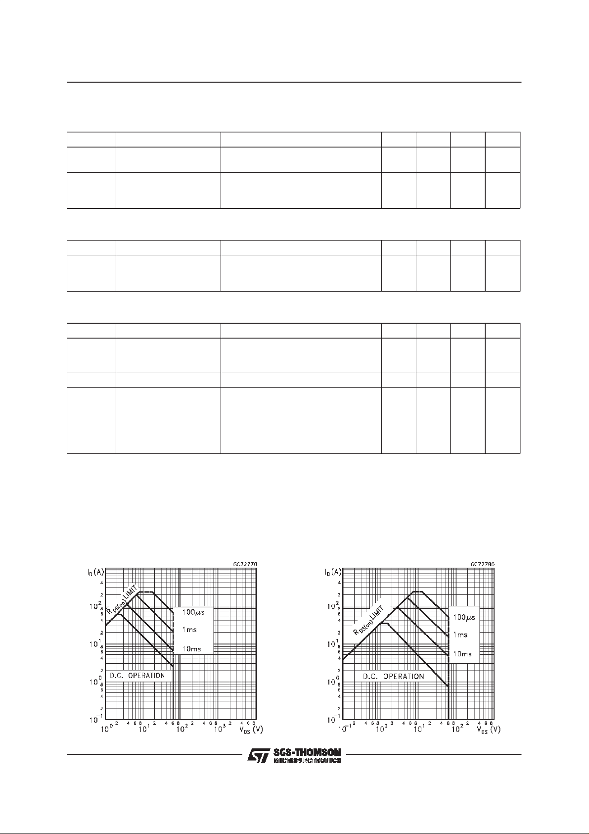
Safe Operating Areafor TO-220 Safe Operating Area for TO-220FP
3/9
 Loading...