

SGS Thomson Microelectronics STP5NB40FP, STP5NB40 Datasheet
STP5NB40
STP5NB40FP
N - CHANNEL ENHANCEMENT MODE
PowerMESH MOSFET
PRELIMINARY DATA
TYPE V
STP5NB40
STP5NB40FP
■ TYPICALR
■ 100% AVALANCHETESTED
■ VERYLOW INTRINSICCAPACITANCES
■ GATECHARGEMINIMIZED
■ EXTREMELY HIGH dv/dt CAPABILITY
DS(on)
DSS
400 V
400 V
=1.47 Ω
R
DS(on)
<1.8Ω
<1.8Ω
I
D
4.7 A
3.1 A
DESCRIPTION
Using the latest high voltage MESH OVERLAY
process, SGS-Thomson has designed an
advanced family of Power MOSFETs with
outstanding performance. The new patent
pending strip layout coupled with the Company’s
proprietary edge termination structure, gives the
lowest RDS(on) per area, exceptional avalanche
and dv/dt capabilities and unrivalled gate charge
and switching characteristics.
APPLICATIONS
■ HIGH CURRENT, HIGH SPEEDSWITCHING
■ SWITCHMODEPOWER SUPPLIES(SMPS)
■ DC-ACCONVERTERS FOR WELDING
EQUIPMENTAND UNINTERRUPTIBLE
POWERSUPPLIESAND MOTORDRIVE
3
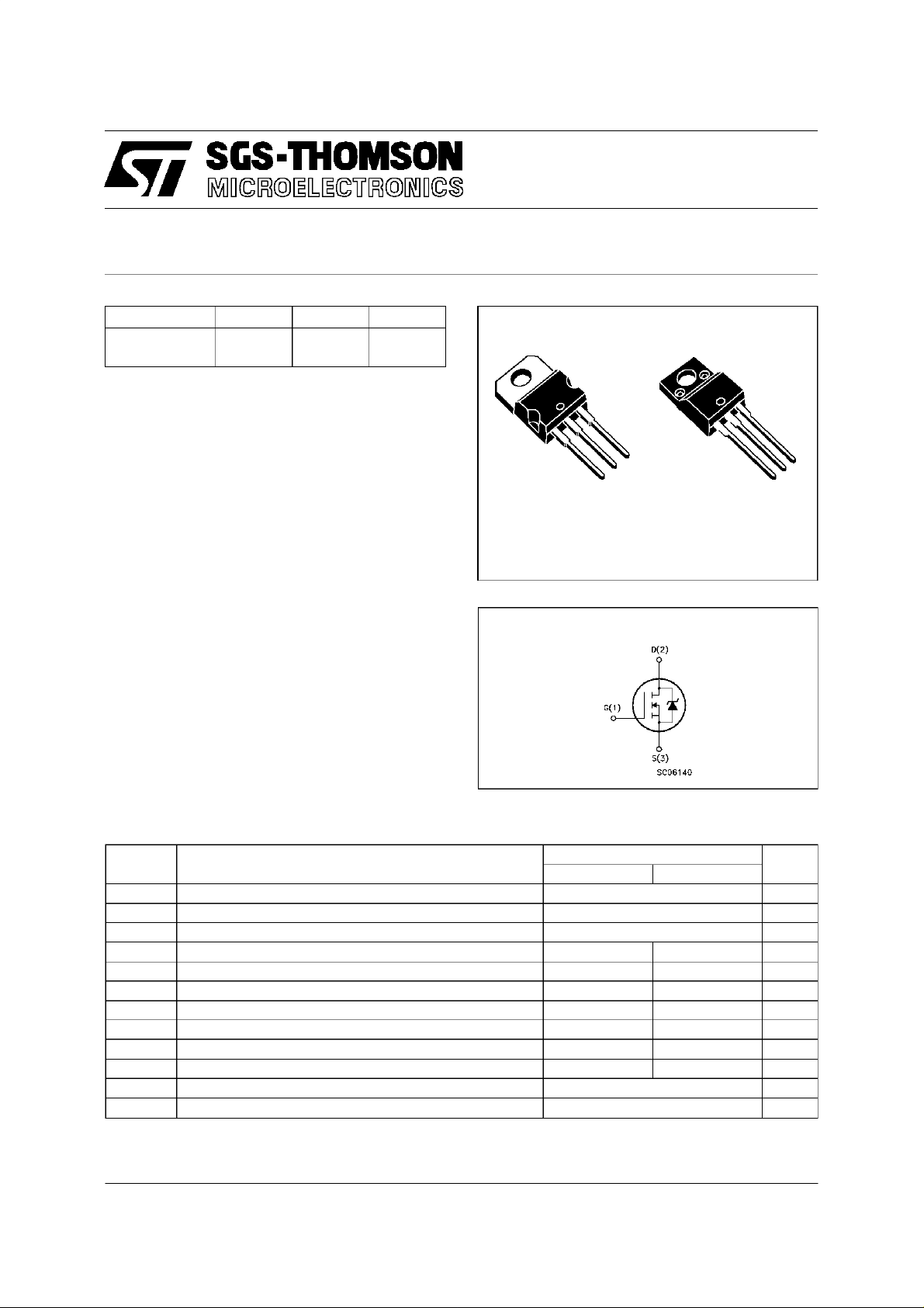
2
1
TO-220 TO-220FP
INTERNAL SCHEMATIC DIAGRAM
3
2
1
ABSOLUTE MAXIMUM RATINGS
Symb o l Para meter Value Uni t
ST P5 NB40 ST P5NB 40FP
V
V
V
I
DM
P
dv/dt(
V
T
(•) Pulse width limitedby safe operating area (1)ISD≤ 5A, di/dt ≤ 200 A/µs, VDD≤ V
October 1997
This ispreliminary information on a new productnow in development or undergoing evaluation. Details are subject to changewithout notice.
Drain-source V oltage (VGS=0) 400 V
DS
Drain- gate Voltage (RGS=20kΩ)
DGR
Gat e- source Voltage ± 30 V
GS
I
Drain Current (cont in uous) a t Tc=25oC4.73.1A
D
I
Drain Current (cont in uous) a t Tc=100oC32A
D
400 V
(•) Drain Cur rent (pulsed) 19 19 A
Tot al D iss ip at ion at Tc=25oC8035W
tot
Derat in g Fac tor 0.64 0.28 W/
1) Peak Diode Recovery v o lt age sl ope 4.5 4.5 V/ns
Ins ulation W it hsta nd V oltage (DC) 2000 V
ISO
Sto rage Temper ature -65 to 150
stg
T
Max. Operat in g J unctio n Te m peratur e 150
j
(BR)DSS
,Tj≤T
JMAX
o
C
o
C
o
C
1/7
STP5NB40/FP
THERMAL DATA
TO-220 TO220-FP
R
thj-case
R
thj-amb
R
thc-sin k
T
AVALANCHE CHARACTERISTICS
Symbol Para met e r Max Value Uni t
I
AR
E
Ther mal Resist ance Junction- case Max 1.56 3.57
Ther mal Resist ance Junction- ambient Max
Ther mal Resist ance Case-sink T y p
Maximum Lea d Temperature Fo r Soldering P urp os e
l
Avalanche Curre nt , Repetit ive or Not - Re petitive
(pulse width limited by T
Single Pulse Avalanche Energy
AS
(starting T
=25oC, ID=IAR,VDD=50V)
j
max, δ <1%)
j
62.5
0.5
300
4.7 A
200 mJ
o
C/W
o
C/W
o
C/W
o
C
ELECTRICAL CHARACTERISTICS (T
=25oC unlessotherwise specified)
case
OFF
Symbol Parameter Te st Cond ition s Min. Typ. M ax. Unit
V
(BR)DSS
Drain-sourc e
=250µAVGS=0V
I
D
400 V
Breakdown Voltage
I
DSS
I
GSS
Zer o Gate Vo lt age
Drain Cur rent (V
GS
Gat e-body Le akage
Current (V
DS
=0)
=0)
=MaxRating
V
DS
V
=MaxRating Tc=125oC
DS
= ± 30 V
V
GS
1
50
± 100 nA
ON (∗)
Symbol Parameter Te st Cond ition s Min. Typ. M ax. Unit
V
GS(th )
Gate Threshold
V
DS=VGSID
=250µA
345V
Voltage
R
DS(on)
Stati c D rain-source On
VGS=10V ID= 2.3 A 1.47 1.8 Ω
Resistance
I
D(on)
On St at e D rain Cu r re nt VDS>I
D(on)xRDS(on)max
4.7 A
VGS=10V
DYNAMIC
Symbol Parameter Te st Cond ition s Min. Typ. M ax. Unit
g
(∗)Forward
fs
Tr ansconductanc e
C
C
C
Input Capaci t an ce
iss
Out put C apa c itance
oss
Reverse T rans fer
rss
Capa cit an c e
VDS>I
D(on)xRDS(on)maxID
=2.3A 1.3 2.4 S
VDS=25V f=1MHz VGS= 0 V 405
72
9
526
94
12
µA
µA
pF
pF
pF
2/7
STP5NB40/FP
ELECTRICAL CHARACTERISTICS (continued)
SWITCHINGON
Symbol Parameter Te st Cond ition s Min. Typ. M ax. Unit
t
d(on)
Turn-on T ime
r
Rise T ime
t
VDD=200V ID=2.3A
=4.7 Ω VGS=10V
R
G
11
8
(see test circuit, figure 3)
Q
Q
Q
Total Gate Charge
g
Gat e-Sour ce Charge
gs
Gate-Drain Charge
gd
VDD=320V ID=4.7A VGS= 1 0 V 14.5
7
5.1
SWITCHINGOFF
Symbol Parameter Te st Cond ition s Min. Typ. M ax. Unit
t
r(Voff)
t
t
Of f - voltage Rise T im e
Fall Time
f
Cross-ov er Tim e
c
VDD=320V ID=4.7A
=4.7 Ω VGS=10V
R
G
(see test circuit, figure 5)
9
6
14
SOURCE DRAIN DIODE
Symbol Parameter Te st Cond ition s Min. Typ. M ax. Unit
I
SD
I
SDM
V
SD
t
Q
I
RRM
(∗) Pulsed: Pulse duration =300 µs, duty cycle1.5 %
(•) Pulse width limited by safe operating area
Source-drain Current
(•)
Source-drain Current
(pulsed)
(∗) For ward On V o lt age ISD=4.7 A VGS=0 1.6 V
Reverse R ecovery
rr
Time
Reverse R ecovery
rr
=4.7 A di/dt = 100 A/µs
I
SD
=100V Tj=150oC
V
DD
(see test circuit, figure 5)
300
1.6
Charge
Reverse R ecovery
10.5
Current
17
12
22 nC
13
10
20
4.7
19
ns
ns
nC
nC
ns
ns
ns
A
A
ns
µC
A
3/7
 Loading...