

SGS Thomson Microelectronics STP5NA80FP Datasheet
N - CHANNEL ENHANCEMENT MODE
FAST POWER MOS TRANSISTOR
TYPE V
DSS
STP5NA80FP 800 V < 2.4 Ω 2.8 A
R
DS(on)
I
D
STP5NA80FP
PRELIMINARY DATA
■ TYPICALR
■ ± 30V GATE TO SOURCE VOLTAGERATING
■ 100% AVALANCHETESTED
■ REPETITIVEAVALANCHEDATAAT 100
■ LOWINTRINSICCAPACITANCES
■ GATECHARGEMINIMIZED
■ REDUCEDTHRESHOLD VOLTAGESPREAD
DS(on)
=1.8 Ω
o
C
DESCRIPTION
This series o f POWER MOSFETS
represents the most advanced high voltage
technology.The optmized celllayout
coupled with a new proprietary edge
termination concur to give the device low
RDS(on) and gate charge, u nequalled
ruggedness and superior switching
performance.
APPLICATIONS
■ HIGH CURRENT, HIGH SPEEDSWITCHING
■ SWITCHMODE POWER SUPPLIES (SMPS)
■ DC-ACCONVERTERS FOR WELDING
EQUIPMENTANDUNINTERRUPTIBLE
POWERSUPPLIESAND MOTOR DRIVE
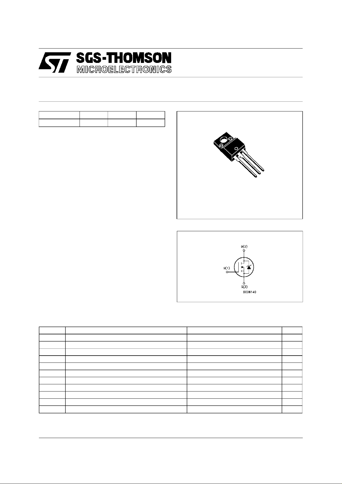
3
2
1
TO-220FP
INTERNAL SCHEMATIC DIAGRAM
ABSOLUTE MAXIMUM RATINGS
Symb o l Parame t er Value Uni t
V
V
DGR Drain- gate Voltage (R
V
I
DM
P
V
T
(•) Pulse width limited by safe operating area
October 1997
Drain-source Voltage (VGS=0) 800 V
DS
=20kΩ)
GS
Gate-sourc e Voltage ± 30 V
GS
I
Drain Current (c ont inuo us) a t Tc=25oC2.8A
D
I
Drain Current (c ont inuo us) a t Tc=100oC1.8A
D
800 V
(•) Drain Current (puls ed) 19 A
Total Dissipat i on at Tc=25oC40W
tot
Derat ing Factor 0.32 W/
Insul at ion W ithst and Voltage (DC) 2000 V
ISO
Stora ge Temperatu re -65 to 15 0
stg
T
Max. Operat ing Junc t i on Temperatu r e 150
j
o
C
o
C
o
C
1/5
STP5NA80FP
THERMAL DATA
R
thj-case
R
thj-amb
R
thc-sin k
T
AVALANCHE CHARACTERISTICS
Symb o l Para met er Max Val ue Uni t
I
AR
E
Ther mal Resistance Junct ion-cas e Max
Ther mal Resistance Junct ion-ambient Max
Ther mal Resistance Case-s i nk Typ
Maximum Lead Temperat ure For Solder in g P urpos e
l
Avalanche Current, Repetitiv e or Not-Repe t it ive
(pulse width lim i t ed by T
Single Pu lse Avalanc he E nerg y
AS
(starti ng T
=25oC, ID=IAR,VDD=50V)
j
max, δ <1%)
j
3.12
62.5
0.5
300
4.7 A
110 mJ
o
C/W
oC/W
o
C/W
o
C
ELECTRICAL CHARACTERISTICS (T
=25oC unlessotherwise specified)
case
OFF
Symbol Parameter Test Cond ition s Min. Typ. Max. Un it
V
(BR)DSS
Drain-source
= 250 µAVGS=0
I
D
800 V
Break dow n Voltage
I
I
DSS
GSS
Zero Gate Voltage
Drain Current (V
GS
Gat e- bod y Leaka ge
Current (V
DS
=0)
=0)
=MaxRating
V
DS
V
=MaxRating Tc= 100oC
DS
= ± 30 V
V
GS
25
250
± 100 nA
ON (∗)
Symbol Parameter Test Cond ition s Min. Typ. Max. Un it
V
GS(th )
R
DS(on)
Gat e Thre shold Volt age
St at ic Drain-source On
V
DS=VGSID
=250µA
VGS= 10V ID= 2.5 A 1.8 2.4 Ω
2.25 3 3.75 V
Resistance
I
D(on)
On State Drain Current VDS>I
D(on)xRDS(on)max
4.7 A
VGS=10V
DYNAMIC
Symbol Parameter Test Cond ition s Min. Typ. Max. Un it
g
(∗)Forward
fs
Tr ansc on ductance
C
C
C
Input Capac it an ce
iss
Out put Capac itance
oss
ReverseTransfer
rss
Capacit a nc e
VDS>I
D(on)xRDS(on)maxID
=2.5A 2.7 5.2 S
VDS=25V f=1MHz VGS= 0 1250
140
35
1700
190
50
µA
µA
pF
pF
pF
2/5
 Loading...