

SGS Thomson Microelectronics STP55NF06LFP, STP55NF06L, STB55NF06L-1, STB55NF06L Datasheet
STP55NF06L - STP55NF06LFP
STB55NF06L - STB55NF06L-1
N-CHANNEL 60V - 0.014Ω - 55A TO-220/FP/D2PAK/I2PAK
STripFET™II POWER MOSFET
TYPE V
STP55NF06L
STP55NF06LFP
STB55NF06L
STB55NF06L-1
■ TYPICAL R
■ EXCEPTIONAL dv/dt CAPABILITY
■ APPLICATION ORIENTED
DS
DSS
60 V
60 V
60 V
60 V
(on) = 0.014Ω
R
DS(on)
<0.018 Ω
<0.018 Ω
<0.018 Ω
<0.018 Ω
I
D
55 A
55 A
55 A
55 A
CHARACTERIZATION
DESCRIPTION
This Power Mosfet is the latest development of
STMicroelectronics unique “Single Feature
™” strip-based process. The re sulting tran-
Size
sistor shows extremely high packing density for
low on-resistance, rugged avalance characteristics and less critical alignment steps therefore a remarkable manufacturing reproducibility.
APPLICATIONS
■ HIGH CURRENT, HIGH SPEED SWITCHING
■ MOTOR CONTROL, AUDIO AMPLIFIERS
■ DC-DC & DC-AC CONVERTERS
■ AUTOMOTIVE ENVI R ONM EN T (IN JECTION,
ABS, AIR-BAG, LAMPDRIVERS, Etc.)
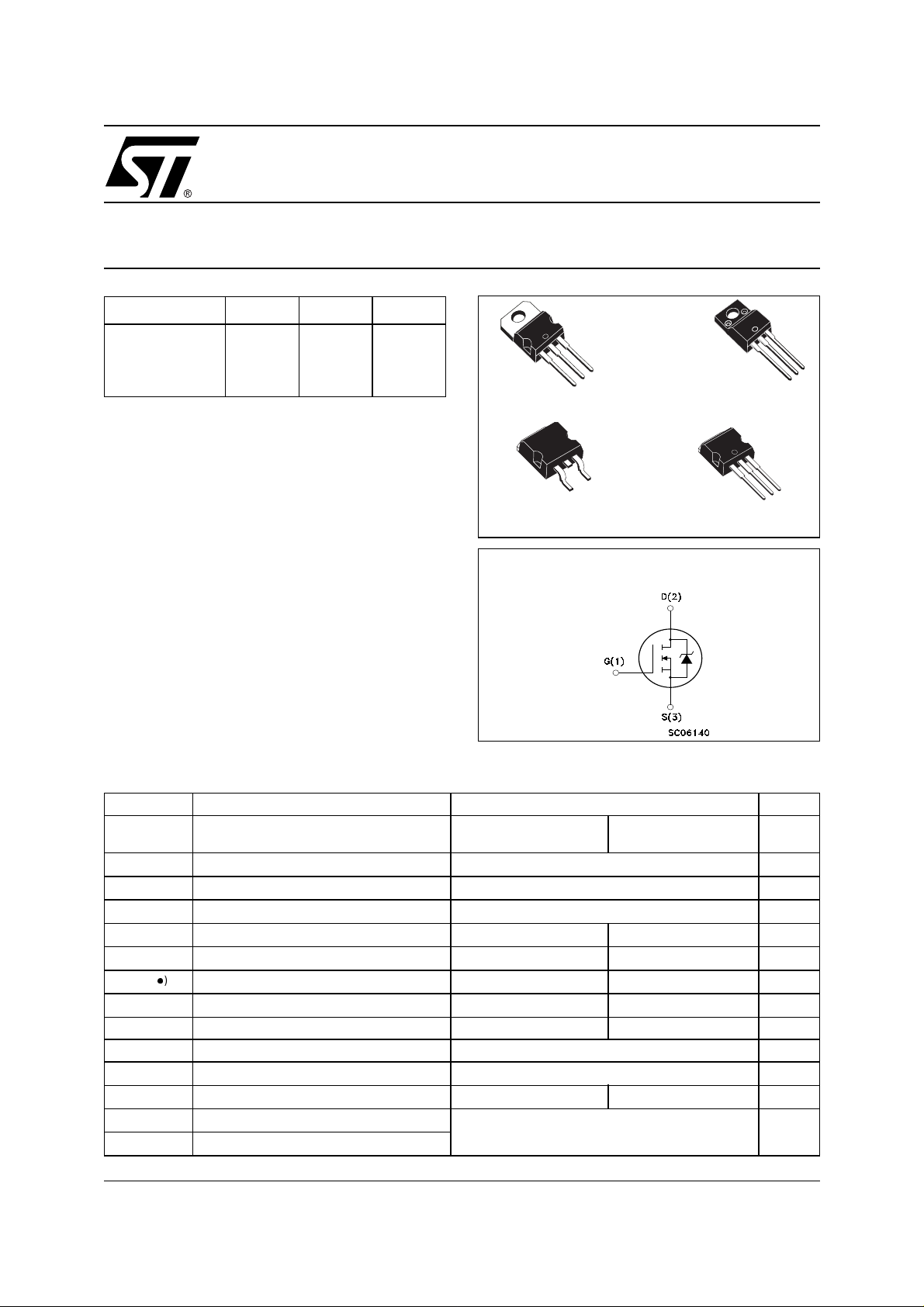
3
2
1
TO-220
2
D
PAK
3
1
TO-220FP
I2PAK
INTERNAL SCHEMATIC DIAGRAM
3
2
1
3
2
1
ABSOLUTE MAXIMUM RATINGS
Symbol Parameter Value Unit
STP55NF06L
STB55NF06L/-1
Drain-source Voltage (VGS = 0)
Drain-gate Voltage (RGS = 20 kΩ)
Gate- source Voltage ± 16 V
Drain Current (continuous) at TC = 25°C
Drain Current (continuous) at TC = 100°C
(l)
Drain Current (pulsed) 220 120 A
Total Dissipation at TC = 25°C
55 30 A
39 21 A
95 30 W
V
I
DM
P
V
DGR
V
I
I
TOT
DS
GS
D
D
Derating Factor 0.63 0.2 W/°C
dv/dt (2) Peak Diode Recovery voltage slope 20 V/ns
(1)
E
AS
V
ISO
T
stg
T
j
(●) Pulse width limited by safe operating area
Single Pulse Avalanche Energy 300 mJ
Insulation Withstand Voltage (DC) - 2500 V
Storage Temperature
Max. Operating Junction Temperature
(1) Starting Tj=25°C, ID=27.5A, VDD=30V
≤ 55 A, di/dt ≤ 200A/µs, VDD ≤ V
(2) I
SD
– 55 to 175 °C
STP55NF06LFP
60 V
60 V
, Tj ≤ T
(BR)DSS
JMAX.
1/12August 2002
STP55NF06L - STP55NF06LFP - STB 55NF06L - STB55NF06L-1
THERMA L D ATA
TO-220
2
PAK
D
2
I
PAK
Rthj-case Thermal Resistance Junction-case Max 1.58 5.0 °C/W
Rthj-amb Thermal Resistance Junction-ambient Max 62.5 °C/W
T
l
Maximum Lead Temperature For Soldering Purpose
ELECTRICAL CHARACTERISTICS (TCASE = 25 °C UNLESS OTHERWISE SPECIFIED)
OFF
Symbol Parameter Test Conditions Min. Typ. Max. Unit
V
(BR)DSS
I
DSS
I
GSS
(1)
ON
Symbol Parameter Test Conditions Min. Typ. Max. Unit
V
GS(th)
R
DS(on)
Drain-source
Breakdown Voltage
Zero Gate Voltage
Drain Current (V
GS
= 0)
Gate-body Leakage
Current (V
DS
= 0)
Gate Threshold Voltage
Static Drain-source On
Resistance
ID = 250 µA, VGS = 0 60 V
V
= Max Rating
DS
V
= Max Rating, TC = 125 °C
DS
V
= ± 16 V ±100 nA
GS
V
= VGS, ID = 250 µA
DS
1 1.7 V
VGS = 5 V, ID = 27.5 A
VGS = 10V, ID = 27.5 A
TO-220FP
300 °C
1µA
10 µA
0.016 0.020 Ω
0.014 0.018 Ω
DYNAMIC
Symbol Parameter Test Conditions Min. Typ. Max. Unit
(1)
g
fs
C
iss
C
oss
C
rss
Forward Transconductance
Input Capacitance
Output Capacitance 300 pF
Reverse Transfer
Capacitance
VDS = 15V , ID = 27.5 A
V
= 25V, f = 1 MHz, VGS = 0
DS
30 S
1700 pF
105 pF
2/12
STP55NF06L - STP55NF06LF P - S TB55NF06L - STB55NF06L-1
ELECTRICAL CHARACTERISTICS (CONTINUED)
SWITCHING ON
Symbol Parameter Test Conditions Min. Typ. Max. Unit
V
t
d(on)
Q
Q
Q
t
r
g
gs
gs
Turn-on Delay Time
Rise Time 100 ns
Total Gate Charge
Gate-Source Charge
Gate-Drain Charge
SWITCHING OFF
Symbol Parameter Test Conditions Min. Typ. Max. Unit
t
d(off)
t
f
Turn-off-Delay Time
Fall Time
SOURCE DRAIN DIODE
Symbol Parameter Test Conditions Min. Typ. Max. Unit
I
SD
I
SDM
VSD (1)
t
rr
Q
rr
I
RRM
Note: 1. Pulsed: Pu l se duration = 300 µs, dut y c yc l e 1.5 %.
2. Pulse width li mited by safe operating area.
Source-drain Current 55 A
(2)
Source-drain Current (pulsed) 220 A
Forward On Voltage
Reverse Recovery Time
Reverse Recovery Charge
Reverse Recovery Current
= 30 V, ID = 27.5A
DD
RG= 4.7Ω VGS = 10V
(see test circuit, Figure 3)
= 48 V, ID = 55 A,
V
DD
VGS = 4.5V
VDD = 30 V, ID = 27.5 A,
RG=4.7Ω, V
GS
= 4.5V
(see test circuit, Figure 5)
ISD = 55 A, VGS = 0
= 55A, di/dt = 100A/µs,
I
SD
VDD = 30 V, Tj = 150°C
(see test circuit, Figure 5)
20 ns
27
37 nC
7
10
40
20
1.3 V
80
200
5
nC
nC
ns
ns
ns
nC
A
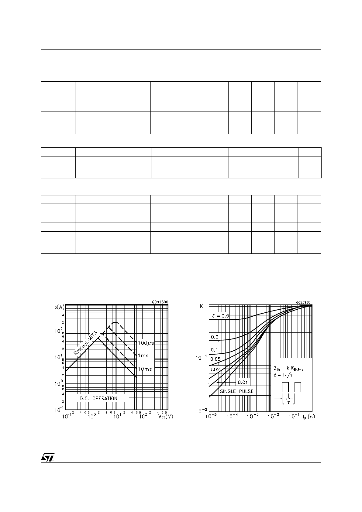
Thermal Impedance for TO-220/D2PAK/I2PAKSafe Operating Area For TO-220/D2PAK/I2PAK
3/12
STP55NF06L - STP55NF06LFP - STB 55NF06L - STB55NF06L-1
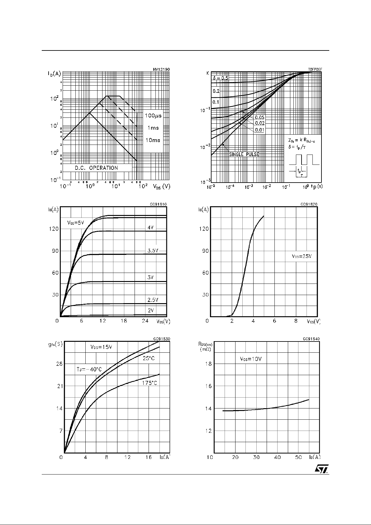
Safe Operating Area For TO-220FP
Output Characteristics
Thermal Impedance For TO-220FP
Transfer Characteristics
Transconductance
4/12
Static Drain-source On Resistance
 Loading...