

SGS Thomson Microelectronics STP55NF06FP, STP55NF06, STB55NF06-1 Datasheet
STB55NF06 STB55NF06-1
STP55NF06 STP55NF06FP
N-CHANNEL 60V - 0.015 Ω - 50A TO-220/ TO-220FP/I²PAK/D²PAK
STripFET™ II POWER MOSFET
TYPE
STP55NF06
STB55NF06-1
STB55NF06
STP55NF06FP
■ TYPICAL R
■ EXCEPTIONA L dv/d t CAPABILITY
■ 100% AVALANCHE TESTED
■ SURFACE-MOUNTING D
V
DSS
60 V
60 V
60 V
60 V
(on) = 0.015 Ω
DS
R
DS(on)
<0.018
Ω
<0.018
Ω
<0.018
Ω
<0.018
Ω
2
PAK (TO-263)
I
D
50 A
50 A
50 A
50 A(*)
POWER PACKAG E IN TU BE (NO SU FFIX) OR
IN TAPE & REEL (SUFFIX “T4”)
■ THROUGH-HOLE I²PAK (TO-262) POWER
PACKAGE IN TUBE (SUFFIX “- 1 ")
DESCRIPTION
This Power MOSFET is th e latest d evelopment of ST-
Microelectronis unique "Single Feature Size™" stripbased process. The resulting transistor shows extremely high packing density for low on-resistance,
rugged avalanche characteristics and less critical
alignment steps therefore a remarkable manufacturing reproducibility.
APPLICATIONS
■ HIGH CURRENT, HIGH SWITCHING SPEED
■ MOTOR CONTROL, AUDIO AMPLIFIERS
■ DC-DC & DC-AC CONVERTERS
■ AUTOMOTIVE
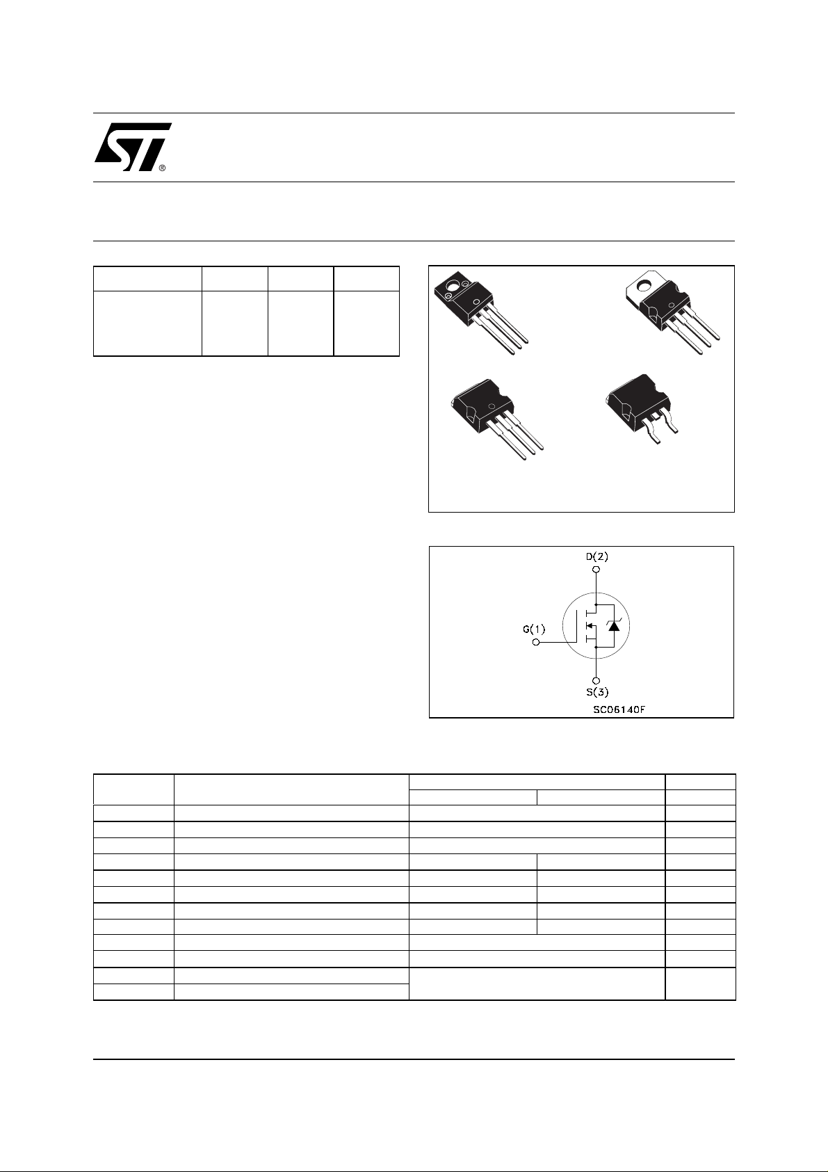
TO-220FP
1
²
PAK
I
TO-262
(Suffix “-1”)
3
2
3
2
1
TO-220
D²PAK
TO-263
(Suffix “T4”)
INTERNAL SCHEMATIC DIAGRAM
3
2
1
3
1
ABSOLUTE MAXIMUM RATINGS
Symbol Parameter Value Unit
STP_B55NF06(-1) STP55NF06FP
V
DS
V
DGR
V
GS
I
D
I
D
(
I
DM
P
tot
dv/dt
E
AS
T
stg
T
j
(
Pulse widt h l i m i ted by safe operating area
•)
(*)Refer to soa for the max allowable current value on FP-type due
to Rth value
.
Drain-source Voltage (VGS = 0)
Drain-gate Voltage (RGS = 20 kΩ)
60 V
60 V
Gate- source Voltage ± 20 V
Drain Current (continuous) at TC = 25°C
Drain Current (continuous) at TC = 100°C
•)
Drain Current (pulsed) 200 200(*) A
Total Dissipation at TC = 25°C
50 50(*) A
35 35(*) A
110 30 W
Derating Factor 0.73 0.2 W/°C
(1)
Peak Diode Recovery voltage slope 7 V/ns
(2)
Single Pulse Avalanche Energy 350 mJ
Storage Temperature
Operating Junction Temperature
(1)
ISD ≤50A, di/dt ≤400A/µs , VDD ≤ V
(2) Starting
-55 to 175 °C
Tj = 25 oC, ID = 25A, VDD= 30V
(BR)DSS
, Tj ≤ T
JMAX
1/12March 2003
STB50NF06 STB55NF06-1 STP55NF06 ST P55NF06FP
THERMA L D ATA
I²PAK
D²PAK
TO-220
Rthj-case Thermal Resistance Junction-case Max 1.36 5 °C/W
Rthj-amb
T
l
Thermal Resistance Junction-ambient
Maximum Lead Temperature For Soldering Purpose
Max 62.5
(1.6 mm from case, for 10 sec)
TO-220FP
300
°C/W
°C
ELECTRICAL CHARACTERISTICS (T
= 25 °C unless otherwise specified)
case
OFF
Symbol Parameter Test Conditions Min. Typ. Max. Unit
I
= 250 µA, VGS = 0
D
V
= Max Rating
DS
V
= Max Rating TC = 125°C
DS
V
= ± 20 V
GS
60 V
1
10
±100 nA
ON
V
(BR)DSS
I
DSS
I
GSS
(*)
Drain-source
Breakdown Voltage
Zero Gate Voltage
Drain Current (V
GS
Gate-body Leakage
Current (V
DS
= 0)
= 0)
Symbol Parameter Test Conditions Min. Typ. Max. Unit
V
GS(th)
R
DS(on)
Gate Threshold Voltage
Static Drain-source On
= VGS I
DS
V
= 10 V ID = 27.5 A
GS
= 250 µA
D
234V
0.015 0.018
V
Resistance
DYNAMIC
Symbol Parameter Test Conditions Min. Typ. Max. Unit
(*)
g
fs
C
iss
C
oss
C
rss
Forward Transconductance
Input Capacitance
Output Capacitance
Reverse Transfer
Capacitance
V
= 15 V ID= 27.5 A
DS
= 25V, f = 1 MHz, VGS = 0
V
DS
18 S
1530
300
105
µA
µA
Ω
pF
pF
pF
2/12
STB50NF06 STB55NF06-1 STP55NF 06 STP55NF06FP
ELECTRICAL CHARACTERISTICS (continued)
SWITCHING ON
Symbol Parameter Test Conditions Min. Typ. Max. Unit
= 30 V ID = 27.5 A
t
d(on)
Turn-on Delay Time
t
r
Rise Time
V
DD
R
= 4.7 Ω VGS = 10 V
G
(Resistive Load, Figure 3)
Q
g
Q
gs
Q
gd
Total Gate Charge
Gate-Source Charge
Gate-Drain Charge
= 48 V ID= 55 A VGS= 10V
V
DD
SWITCHING OFF
Symbol Parameter Test Conditions Min. Typ. Max. Unit
= 30V ID = 27.5 A
t
d(off)
Turn-off Delay Time
t
f
Fall Time
V
DD
R
= 4.7Ω, V
G
GS
= 10 V
(Resistive Load, Figure 3)
SOURCE DRAIN DIODE
Symbol Parameter Test Conditions Min. Typ. Max. Unit
I
SD
I
SDM
V
SD
t
rr
Q
rr
I
RRM
(*)
Pulsed: P ul se duration = 300 µs, duty cycle 1.5 %.
(
•)Pulse width limited by s af e operating area.
Source-drain Current
(•)
Source-drain Current (pulsed)
(*)
Forward On Voltage
Reverse Recovery Time
Reverse Recovery Charge
Reverse Recovery Current
I
= 55A VGS = 0
SD
= 55 A di/dt = 100A/µs
I
SD
V
= 30 V Tj = 150°C
DD
(see test circuit, Figure 5)
16
8
44.5
10.5
17.5
36
15
75
170
4.5
60 nC
50
200
1.5 V
ns
ns
nC
nC
ns
ns
A
A
ns
nC
A
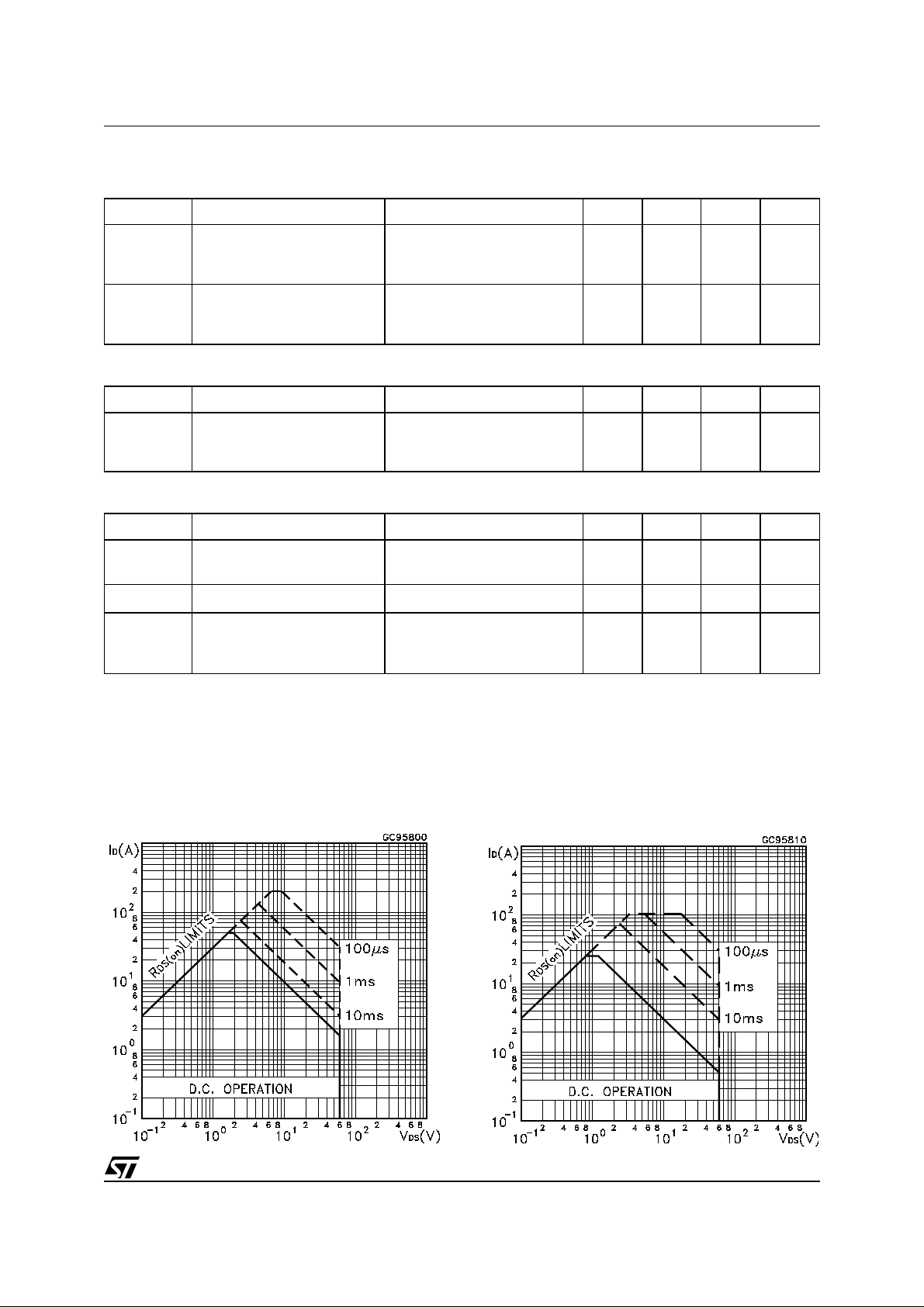
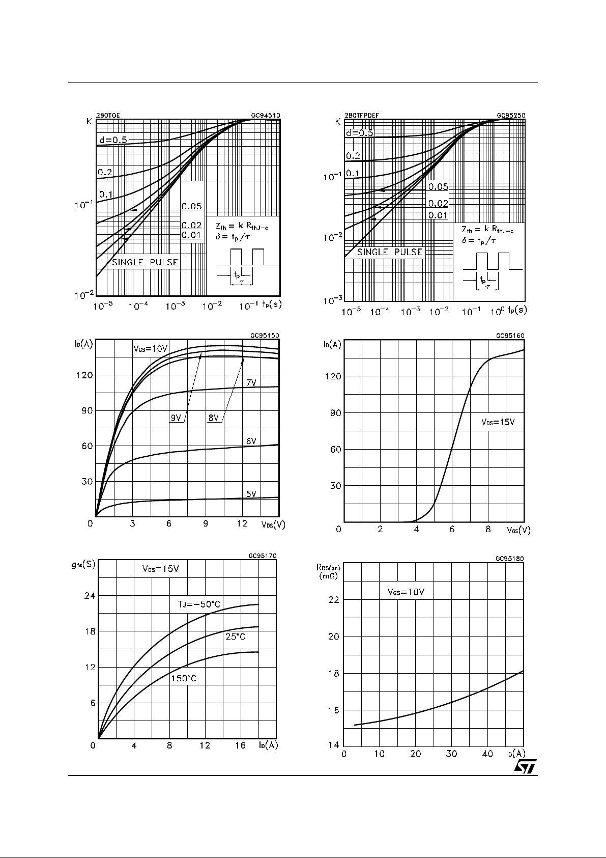
Safe Operating Area for TO-220FPSafe Operating Area for
3/12
STB50NF06 STB55NF06-1 STP55NF06 ST P55NF06FP
Thermal Impedance Thermal Impedance for TO-220FP
Output Characteristics Transfer Characteristics
Transconductance Static Drain-source On Resistance
4/12
 Loading...