

STP55NF03L
N-CHANNEL 30V - 0.01Ω - 55A TO-220
STripFET POWER MOSFET
TYPE
V
DSS
R
DS(on)
I
D
STP55NF03L 30 V <0.013 Ω 55 A
■ TYPICAL RDS(on) = 0.01Ω
■ OPTIMIMIZED FOR HIGH SWITCHING
OPERATIONS
■ LOW GATE CHARGE
■ LOGIC LEVEL GATE DRIVE
DESCRIPTION
This Power MOSFET is the latest development of
STMicroelectronics unique “Single Feature
Size” strip-basedprocess. The resulting transistor shows extremely high packing density for low
on-resistance, rugged avalanche characteristics
and less critical alignment steps therefore a remarkable manufacturing reproducibility.
APPLICATIONS
■ LOW VOLTAGE DC-DC CONVERTERS
■ HIGH CURRENT, HIGHSPEED SWITCHING
■ HIGH EFFICIENCY SWITCHING CIRCUITS
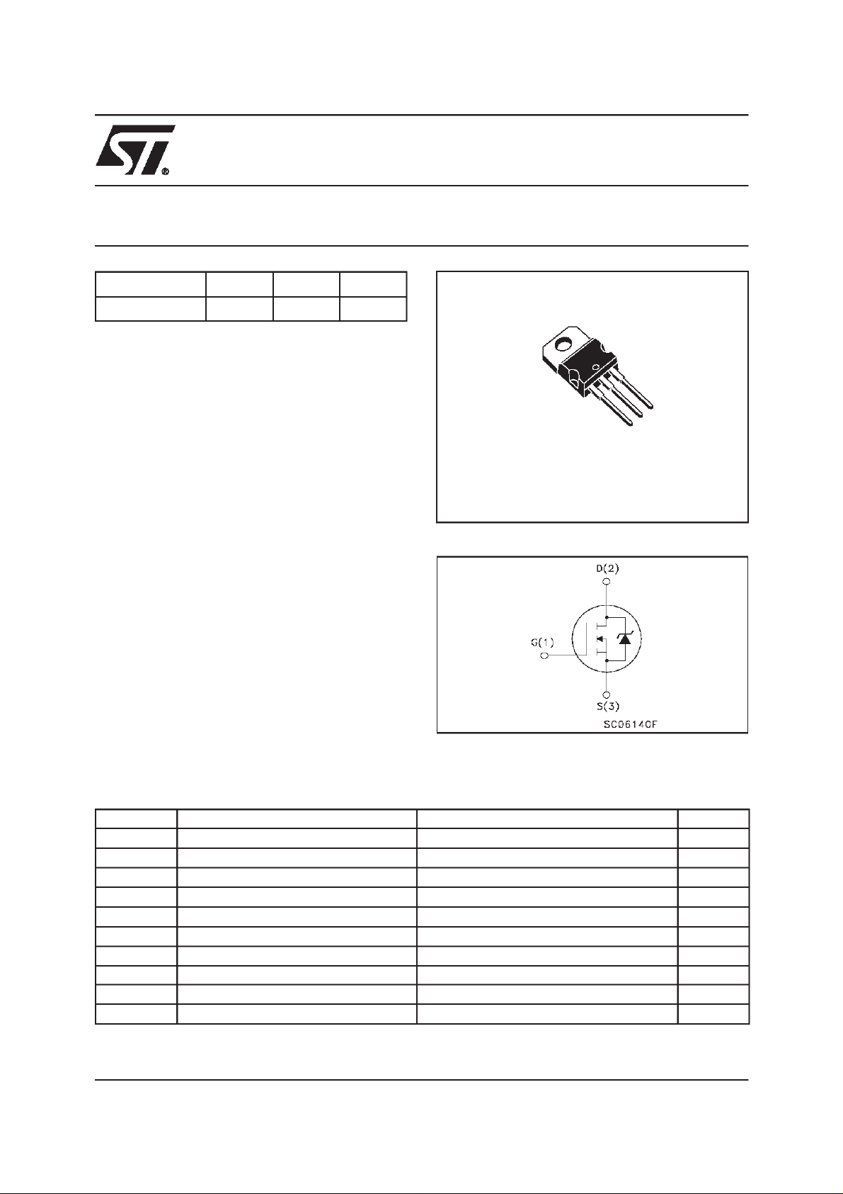
3
2
1
TO-220
INTERNAL SCHEMATIC DIAGRAM
ABSOLUTE MAXIMUM RATINGS
Symbol Parameter Value Unit
V
DS
V
DGR
V
GS
I
D
I
D
(•)
I
DM
P
tot
T
stg
T
j
(•)Pulse width limited by safe operating area.
Drain-source Voltage (VGS=0) 30 V
Drain-gate Voltage (RGS=20kΩ)
30 V
Gate- source Voltage ±15 V
Drain Current (continuos) at TC=25°C
55 A
Drain Current (continuos) at TC= 100°C39 A
Drain Current (pulsed) 220 A
TotalDissipation at TC=25°C
80 W
Derating Factor 0.53 W/°C
Storage Temperature –60 to 175 °C
Max. Operating Junction Temperature 175 °C
1/8February 2001
STP55NF03L
THERMAL DATA
R
thj-case
R
thj-amb
R
thc-sink
T
j
Thermal Resistance Junction-case
Thermal Resistance Junction-ambient
Thermal Resistance Case-sink
Maximum Lead Temperature For Soldering Purpose
Max
Max
Typ
1.875
62.5
0.5
300
°C/W
°C/W
°C/W
°C
ELECTRICAL CHARACTERISTICS (T
=25°C unless otherwise specified)
case
OFF
Symbol Parameter Test Conditions Min. Typ. Max. Unit
ON
V
(BR)DSS
I
DSS
I
GSS
(*)
Drain-source
Breakdown Voltage
Zero Gate Voltage
Drain Current (V
GS
Gate-body Leakage
Current (V
DS
=0)
=0)
ID= 250 µAVGS=0 30 V
V
= Max Rating
DS
=Max Rating TC= 125 °C
V
DS
V
= ±15 V ±100 nA
GS
1
10
Symbol Parameter Test Conditions Min. Typ. Max. Unit
V
GS(th)
R
DS(on)
I
D(on)
Gate Threshold Voltage VDS=V
Static Drain-source On Resis-
tance
VGS=10V ID= 27.5 A
= 4.5 V ID= 27.5 A
V
GS
On State Drain Current VDS>I
VGS=10V
GS
D(on)xRDS(on)max
ID= 250 µA1 V
0.01
0.013
0.013
0.020
55 A
DYNAMIC
Symbol Parameter Test Conditions Min. Typ. Max. Unit
(*)
g
fs
Forward Transconductance VDS>I
ID=27.5 A
D(on)xRDS(on)max
30 S
µA
µA
Ω
Ω
2/8
C
iss
C
oss
C
rss
Input Capacitance
Output Capacitance
Reverse Transfer
Capacitances
= 25V f = 1 MHz VGS= 0 1265
V
DS
435
115
pF
pF
pF
STP55NF03L
ELECTRICAL CHARACTERISTICS (continued)
SWITCHING ON
Symbol Parameter Test Conditions Min. Typ. Max. Unit
t
d(on)
t
Turn-on DelayTime Rise Time VDD=15V ID= 27.5 A
= 4.7 Ω VGS= 4.5 V
r
R
G
(see test circuit, Figure 3)
28
400
ns
ns
Q
g
Q
gs
Q
gd
Total Gate Charge
Gate-Source Charge
Gate-Drain Charge
=24V ID=55A VGS=4.5V 20
V
DD
7
27 nC
10
SWITCHING OFF
Symbol Parameter Test Conditions Min. Typ. Max. Unit
t
d(off)
t
turn-off Delay Time
f
Fall Time
VDD=15V ID= 27.5 A
= 4.7 Ω VGS= 4.5 V
R
G
25
50
(see test circuit, Figure 3)
SOURCE DRAIN DIODE
Symbol Parameter Test Conditions Min. Typ. Max. Unit
I
SD
I
SDM
V
SD
t
rr
Q
rr
I
RRM
(*)Pulsed: Pulse duration = 300 µs, duty cycle 1.5 %.
(•)Pulse width limitedby safe operating area.
Source-drain Current
(•)
Source-drain Current (pulsed)
55
220
(*) Forward On Voltage ISD=55A VGS= 0 1.3 V
Reverse Recovery Time
Reverse Recovery Charge
Reverse Recovery Current
=55 A di/dt = 100A/µs
I
SD
=30V Tj= 150 °C
V
DD
(see test circuit, Figure 5)
70
160
4.5
nC
nC
ns
ns
A
A
ns
nC
A
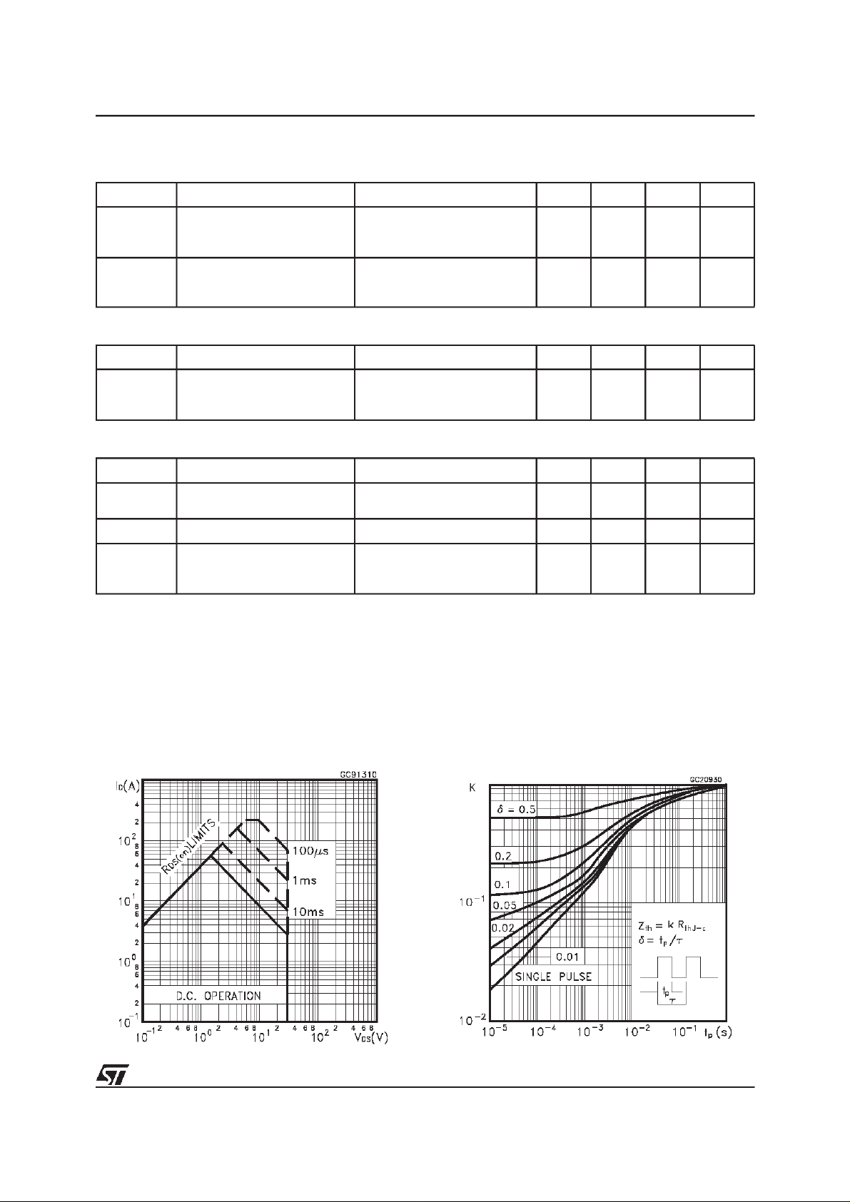
Thermal ImpedanceSafe Operating Area
3/8
 Loading...