

SGS Thomson Microelectronics STP55NE06 Datasheet
STP55NE06
STP55NE06FP
N - CHANNEL ENHANCEMENT MODE
” SINGLE FEATURE SIZE ” POWER MOSFET
TYPE V
STP55NE06
STP55NE06FP
■ TYPICALR
■ EXCEPTIONAL dv/dt CAPABILITY
■ 100% AVALANCHETESTED
■ LOW GATE CHARGE 100
■ HIGH dv/dt CAPABILITY
■ APPLICATIONORIENTED
DS(on)
DSS
60 V
60 V
=0.019 Ω
R
DS(on)
<0.022Ω
<0.022Ω
o
C
I
D
55 A
30 A
CHARACTERIZATION
DESCRIPTION
This Power Mosfet is the latest development of
SGS-THOMSON unique ”Single Feature Size”
strip-based process. The resulting transistor
shows extremelyhigh packing density for low onresistance, rugged avalance characteristics and
less critical alignment steps therefore a remarkable manufacturingreproducibility.
APPLICATIONS
■ DC MOTOR CONTROL
■ DC-DC& DC-AC CONVERTERS
■ SYNCHRONOUS RECTIFICATION
3
2
1
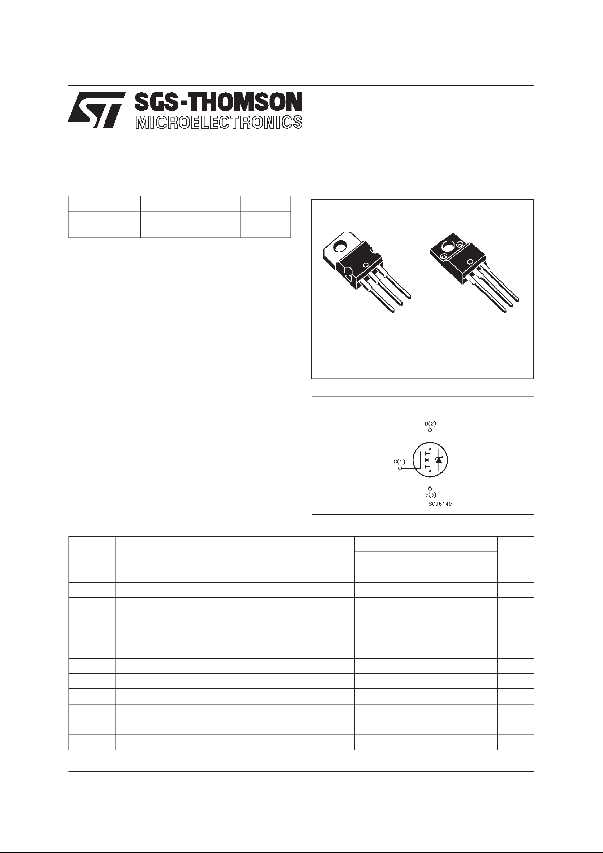
TO-220 TO-220FP
INTERNAL SCHEMATIC DIAGRAM
3
2
1
ABSOLUTE MAXIMUM RATINGS
Symb o l Para meter Value Uni t
STP 55NE06 STP55 NE06F P
V
V
V
I
DM
P
V
dv/ dt Peak Diode Recov ery vo lt age sl ope 7 V/ns
T
(•) Pulsewidth limitedby safe operating area (1)ISD≤ 55 A,di/dt ≤ 300 A/µs, VDD≤ V
January 1998
Drain-source Voltage (VGS=0) 60 V
DS
Drain- gate Voltage ( RGS=20kΩ)
DGR
Gat e- source Volt age ± 20 V
GS
I
Drain Current (c on t in uous) at Tc=25oC5530A
D
I
Drain Current (c on t in uous) at Tc=100oC3921A
D
60 V
(•) Dr a in Curr ent (pul sed) 220 220 A
Tot al Dissip at i on at Tc=25oC13035W
tot
Derat in g F actor 0.96 0.27 W/
Ins ulation With st and Voltage (DC) 2000 V
ISO
Sto rage T emperat ure -65 to 17 5
stg
T
Max. Oper at in g Junc t io n Temperatur e 175
j
(BR)DSS,Tj≤TJMAX
o
C
o
C
o
C
1/9
STP55NE06/FP
THERMAL DATA
TO - 2 20 TO-220FP
R
thj-case
R
thj-amb
R
thc-sin k
T
AVALANCHE CHARACTERISTICS
Symbol Paramet e r Max Va lu e Uni t
I
AR
E
Ther mal Resist ance Junction- case Max 1.15 4.28
Ther mal Resist ance Junction- ambient Max
Ther mal Resist ance Case-sink Ty p
Maximum Lead Tempera t ure For Sold ering Purpose
l
Avalanche Current, Repetit i v e or Not-Repetitive
(pulse w idth limited by T
Single Pulse Avalanche Energy
AS
(starting T
=25oC, ID=IAR,VDD=25V)
j
max, δ <1%)
j
62.5
0.5
300
55 A
200 mJ
o
C/W
o
C/W
o
C/W
o
C
ELECTRICAL CHARACTERISTICS (T
=25oC unlessotherwise specified)
case
OFF
Symbol Parameter Test Cond itions Min. Typ. Max. Unit
V
(BR)DSS
Drain-source
=250µAVGS=0
I
D
60 V
Breakdown Voltage
I
DSS
I
GSS
Zer o Gate Vo lt age
Drain Cur re nt (V
GS
Gat e-body Leakage
Current (V
DS
=0)
=0)
=MaxRating
V
DS
V
=MaxRating Tc=125
DS
o
C
= ± 20 V
V
GS
1
10
± 100 nA
ON (∗)
Symbol Parameter Test Cond itions Min. Typ. Max. Unit
V
GS(th )
Gate Threshold
V
DS=VGSID
=250µA
234V
Voltage
R
DS(on)
Stati c Drain-so urce On
VGS=10V ID= 27.5 A 0.019 0.022 Ω
Resistance
I
D(on)
On State Drain Cu rr e nt VDS>I
D(on)xRDS(on)max
55 A
VGS=10V
DYNAMIC
Symbol Parameter Test Cond itions Min. Typ. Max. Unit
g
(∗)Forward
fs
Tr ansconductance
C
C
C
Input Capaci t ance
iss
Out put Capa citance
oss
Reverse Transfer
rss
Capa cit an c e
VDS>I
D(on)xRDS(on)maxID
=27. 5 A 25 35 S
VDS=25V f=1MHz VGS= 0 3050
380
100
4000
500
130
µA
µA
pF
pF
pF
2/9
STP55NE06/FP
ELECTRICAL CHARACTERISTICS (continued)
SWITCHINGON
Symbol Parameter Test Cond itions Min. Typ. Max. Unit
t
d(on)
t
Q
Q
Q
SWITCHINGOFF
Symbol Parameter Test Cond itions Min. Typ. Max. Unit
t
r(Voff)
t
SOURCE DRAIN DIODE
Symbol Parameter Test Cond itions Min. Typ. Max. Unit
I
SD
I
SDM
V
SD
t
Q
I
RRM
(∗) Pulsed: Pulse duration =300 µs, duty cycle 1.5 %
(•) Pulse widthlimited by safe operating area
r
Turn-on Time
Rise Tim e
VDD=30V ID= 27.5 A
R
=4.7 W VGS=10V
G
30
12040160
(see test circuit, figure 3)
Total Gate Charge
g
Gat e-Sourc e Charge
gs
Gate-Drain Charge
gd
Of f - voltage Rise T im e
t
Fall Time
f
Cross-over Time
c
Source-drain Current
(•)
Source-drain Current
VDD=48V ID=55A VGS=10V 80
13
25
VDD=48V ID=55A
=4.7 Ω VGS=10V
R
G
(see test circuit, figure 5)
20
50
75
105 nC
30
70
100
55
220
(pulsed)
(∗) For ward O n Vo lt age ISD=60A VGS=0 1.5 V
Reverse Recover y
rr
Time
Reverse Recover y
rr
= 55 A di/dt = 100 A /µ s
I
SD
=30V Tj=150oC
V
DD
(see test circuit, figure 5)
110
430
Charge
Reverse Recover y
7.5
Current
ns
ns
nC
nC
ns
ns
ns
A
A
ns
µC
A
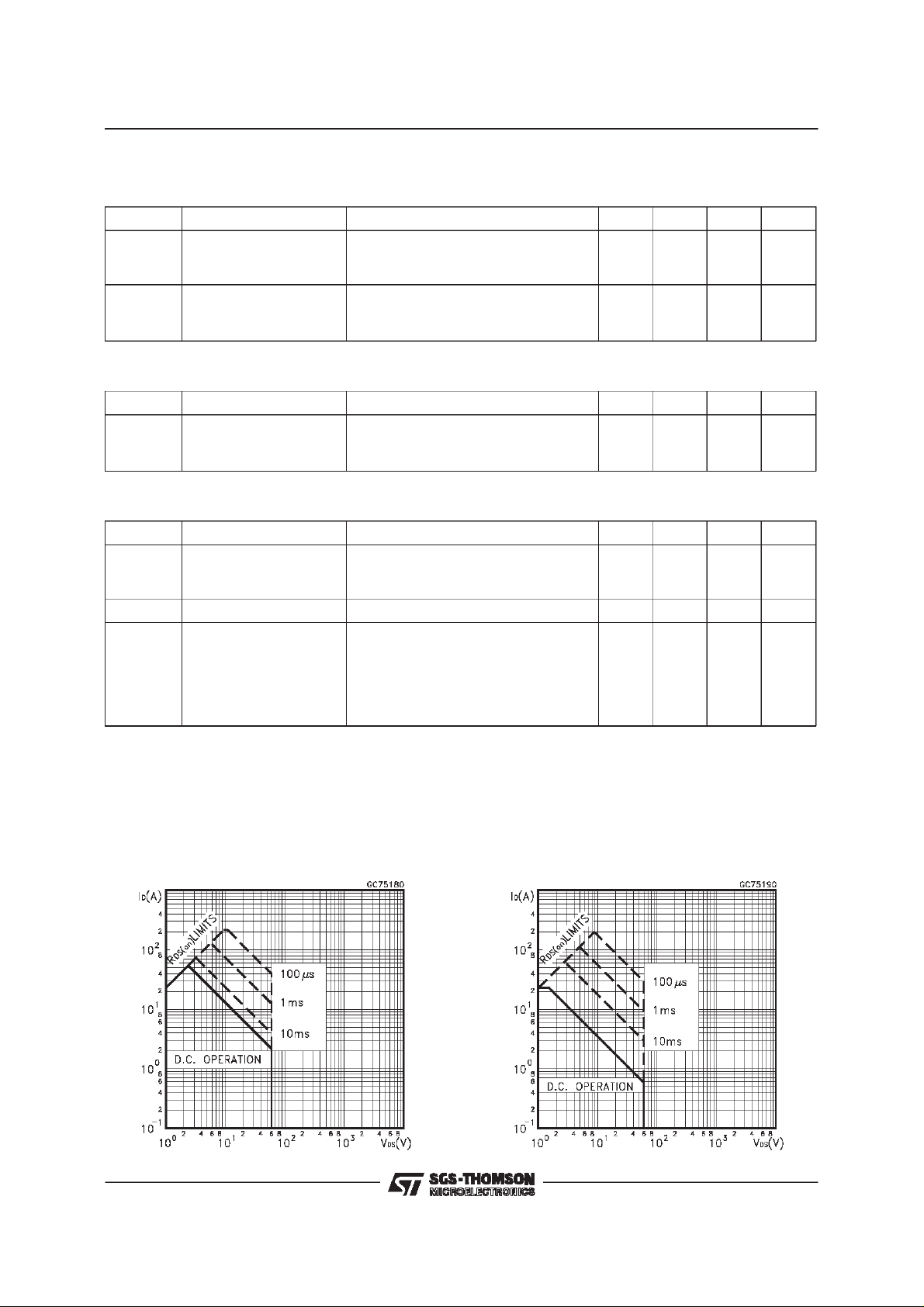
Safe Operating Areafor TO-220 Safe Operating Area for TO-220FP
3/9
 Loading...