

SGS Thomson Microelectronics STP50NE10L Datasheet
STP50NE10L
N - CHANNEL 100V - 0.020Ω - 50A TO-220
STripFET POWER MOSFET
TYPE V
DSS
R
DS(on)
I
D
ST P50NE10L 100 V <0 . 025 Ω 50 A
■ TYPICALR
■ EXCEPTIONALdv/dtCAPABILITY
■ 100%AVALANCHETESTED
■ LOW GATE CHARGE AT100
■ APPLICATIONORIENTED
DS(on)
= 0.020 Ω
o
C
CHARACTERIZATION
DESCRIPTION
This PowerMOSFET is the latest developmentof
STMicroelectronics unique ”Single Feature
Size” strip-based process. The resulting
transistor shows extremely high packing density
for low on-resistance, rugged avalanche
characteristics and less critical alignment steps
therefore a remarkable manufacturing
reproducibility.
APPLICATIONS
■ HIGHCURRENT, HIGH SPEED SWITCHING
■ SOLENOIDAND RELAYDRIVERS
■ MOTORCONTROL, AUDIOAMPLIFIERS
■ DC-DC& DC-ACCONVERTERS
■ AUTOMOTIVEENVIRONMENT(INJECTION,
ABS, AIR-BAG, LAMPDRIVERS,Etc.)
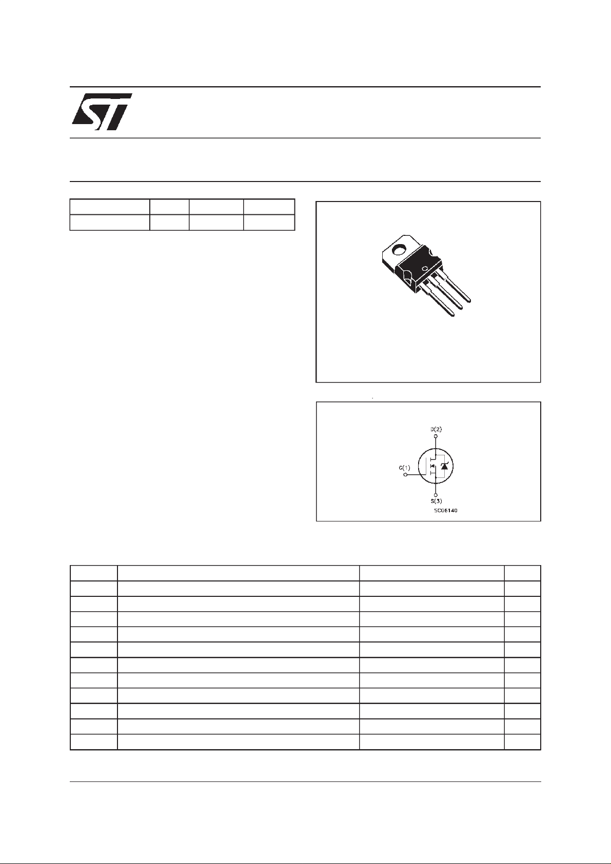
3
2
1
TO-220
INTERNAL SCHEMATIC DIAGRAM
ABSOLUTE MAXIMUM RATINGS
Symbol Parameter Value Unit
V
V
V
I
DM
P
dv/dt (
T
(•) Pulsewidth limited by safeoperating area (1)ISD≤ 50 A, di/dt ≤ 275 A/µs, VDD≤ V
May 1999
Dra in- sour c e Vol t age (VGS= 0) 100 V
DS
Dra in- gate Voltage (RGS=20kΩ) 100 V
DGR
Gat e-source Voltage ± 20 V
GS
I
Dra in Current ( continuous) at Tc=25oC50A
D
I
Dra in Current ( continuous) at Tc=100oC35A
D
(•) D rain Cu rr ent ( p uls ed ) 200 A
Tot al Dissipation at Tc=25oC 150 W
tot
Derating Factor 1 W/
1) Peak Diode Re c overy v olt age slope 6 V/ ns
St orage Tem pe r at ure -65 to 175
stg
T
Max. Operat ing Junct ion Temperature 175
j
(BR)DSS,Tj≤TJMAX
o
C
o
C
o
C
1/8
STP50NE10L
THERMAL DATA
R
thj-case
Rthj-amb
R
thc-sink
T
AVALANCHE CHARACTERISTICS
Symbol Parameter Max Value U nit
I
AR
E
Ther mal Resistanc e Junct ion-case Max
Ther mal Resistanc e Junct ion-ambient Max
Ther mal Resistanc e Case-sink Ty p
Maximum L ead Tempera tur e For Solder ing Purp ose
l
Avalanche Current, Repetitive or Not-Repetitive
(pulse width limited by T
Single Pulse A valanche Energy
AS
(starting T
=25oC, ID=IAR,VDD=50V)
j
max)
j
1
62.5
0.5
300
50 A
400 mJ
o
C/W
oC/W
o
C/W
o
C
ELECTRICAL CHARACTERISTICS
=25oC unless otherwisespecified)
(T
case
OFF
Symbol Parameter Test Conditions Min. Typ. Max. Unit
V
(BR)DSS
Drain-source
ID=250µAVGS= 0 100 V
Break dow n Voltage
I
DSS
I
GSS
Zero Gate Voltage
Drain Current (V
GS
Gat e- bod y Leakage
Current (V
DS
=0)
=0)
V
=MaxRating
DS
=MaxRating Tc= 125oC
V
DS
V
=± 20 V
GS
1
10
100 nA
±
ON(∗)
Symbol Parameter Test Conditions Min. Typ. Max. Unit
V
GS(th)
R
DS(on)
I
D(on)
Gate Threshold Voltage VDS=VGSID= 250 µ A11.72.5V
Sta t ic Drain-sour ce On
Resistance
VGS=10V ID=25A
=5V ID=25A
V
GS
On StateDrain Current VDS>I
D(on)xRDS(on )max
0.020
0.024
50 A
0.025
0.030ΩΩ
VGS=10V
DYNAMIC
Symbol Parameter Test Conditions Min. Typ. Max. Unit
g
(∗)Forward
fs
Tr ansc on duc tance
C
C
C
Input Capacitance
iss
Out put Capacitance
oss
Reverse Transfer
rss
Capacit a nc e
VDS>I
D(on)xRDS(on )maxID
=25 A 45 S
VDS=25V f=1MHz VGS= 0 5000
500
180
µ
µA
pF
pF
pF
A
2/8
STP50NE10L
ELECTRICAL CHARACTERISTICS
(continued)
SWITCHINGON
Symbol Parameter Test Conditions Min. Typ. Max. Unit
t
d(on)
t
Tur n-on Delay Time
Rise Time
r
VDD=50V ID=25A
R
=4.7
G
Ω
VGS=5V
30
105
(Resis t iv e Load, see fig. 3)
Q
Q
Q
Tot al Gate Charge
g
Gat e- Source Char g e
gs
Gate-Drain Charge
gd
VDD=80V ID=50A VGS=5V 82
17
49
105 nC
SWITCHINGOFF
Symbol Parameter Test Conditions Min. Typ. Max. Unit
t
d(off)
Tur n-of f Delay Time
t
Fall T ime
f
VDD=50V ID=25A
=4.7 Ω VGS=5V
R
G
135
45
(Resis t iv e Load, see fig. 3)
t
r(Voff)
t
t
Off-volt age Rise Tim e
Fall T ime
f
Cross-over Time
c
V
=80V ID=50A
clamp
=4.7 Ω VGS=5V
R
G
(Indu ctive Load, see fig. 5)
45
45
85
SOURCE DRAIN DIODE
Symbol Parameter Test Conditions Min. Typ. Max. Unit
I
SD
I
SDM
V
SD
t
Q
I
RRM
(∗) Pulsed: Pulse duration = 300µs, duty cycle 1.5 %
(•) Pulse width limited by safe operating area
Sou rc e-d rai n Cur ren t
(•)
Sou rc e-d rai n Cur ren t
50
200
(pulsed)
(∗)ForwardOnVoltage ISD=50A VGS=0 1.5 V
Reverse Recovery
rr
Time
Reverse Recovery
rr
ISD= 30 A di/dt = 100 A /µs
=50V Tj=150oC
V
DD
(s ee tes t cir cu it, fig . 5)
165
870
Charge
Reverse Recovery
10.5
Current
ns
ns
nC
nC
ns
ns
ns
ns
ns
A
A
ns
nC
A
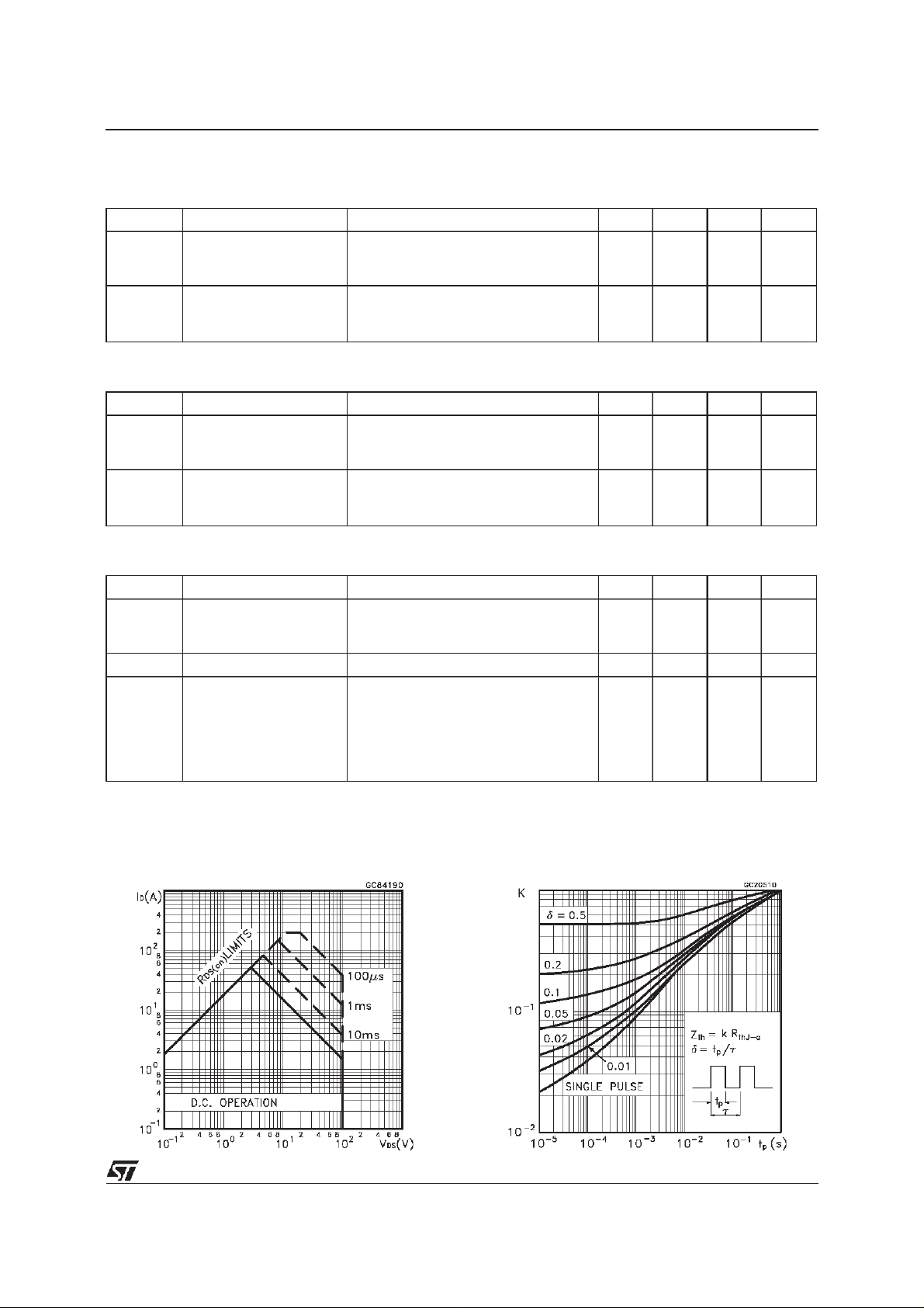
Safe Operating Area Thermal Impedan ce
3/8
 Loading...