

SGS Thomson Microelectronics STP4NC80ZFP, STB4NC80ZT4 Datasheet
1/14November 2003
STP4NC80Z - STP4NC80ZFP
STB4NC80Z - STB4NC80Z-1
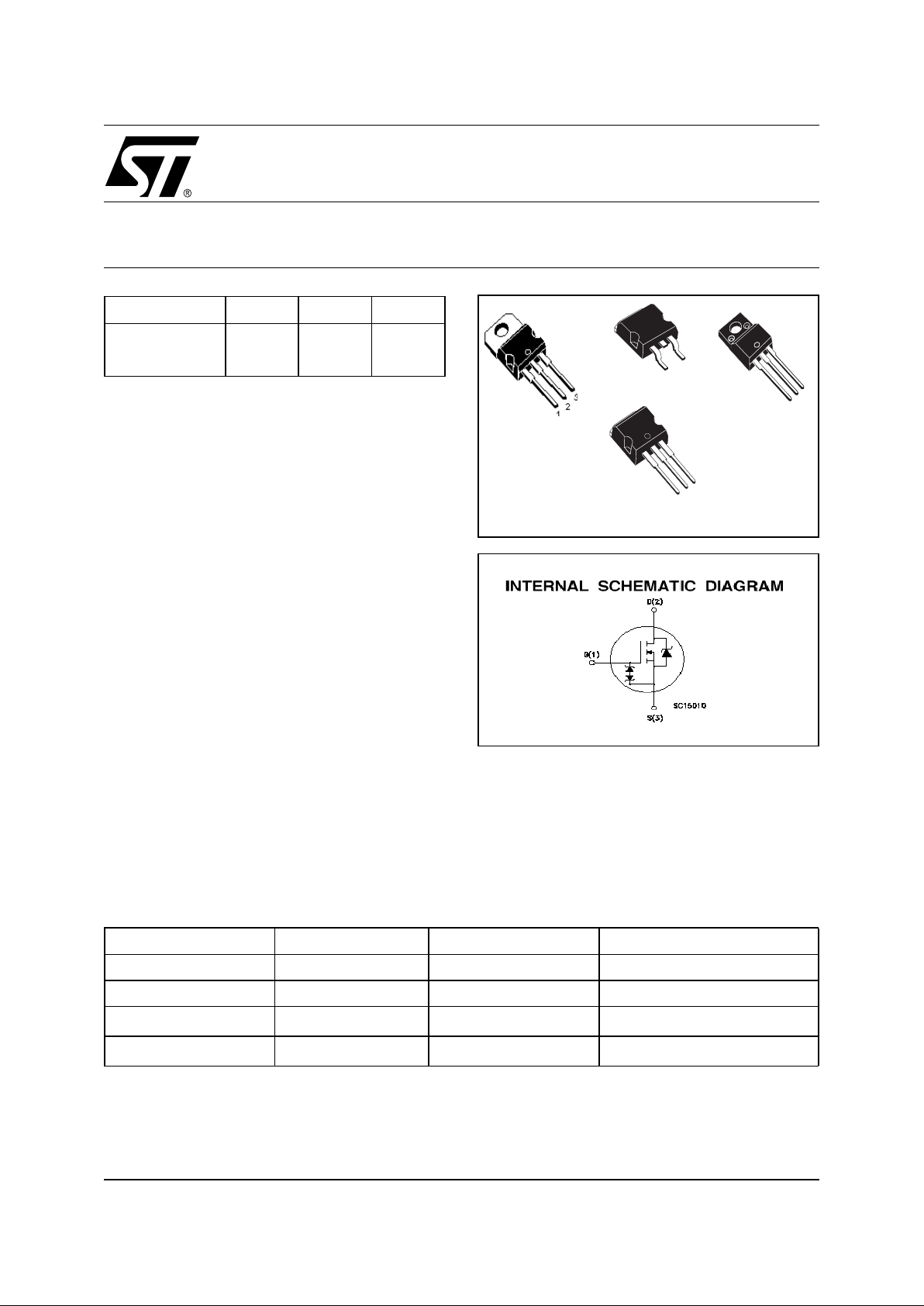
N-CHANNEL 800V - 2.4Ω - 4A TO-220/FP/D2PAK/I2PAK
Zener-Protected PowerMESH™III MOSFET
TO-220
1
2
3
TO-220FP
1
2
3
I2PAK
(Tabless TO-220)
1
3
D2PAK
■ TYPICAL R
DS
(on) = 2.4 Ω
■ EXTREMELY HIGH dv/dtAND CAPABILITY
GATE-TO- SO URCE ZENER DIODES
■ 100% AVALANCHE TESTED
■ V ER Y LOW GATE INPUT RESISTANCE
■ GAT E CHARGE MINIMIZED
DESCRIPTION
The third generation of MESH OVERLAY™ Power
MOSFETs for very high v oltage exhibits unsurpassed on-resistan ce pe r unit area wh ile integrating back-to-back Zener diode s between gat e and
source. Such arrangement gives extra ESD capability with higher ruggedness pe rformanc e as requested by a large variety of single-swit c h
applications.
APPLICATIONS
■ S INGLE -ENDED S MPS IN MONITORS,
COMPUTER AND INDUSTRIAL APPLICATION
■ WELDING EQUIPMENT
ORDERING INFORMATION
TYPE V
DSS
R
DS(on)
I
D
STP4NC80Z/FP 800V < 2.8 Ω 4A
STB4NC80Z/-1 800V < 2.8 Ω 4A
SALES TYPE MARKING PACKAGE PACKAGING
STP4NC80Z P4NC80Z TO-220 TUBE
STP4NC80ZFP P4NC80ZFP TO-220FP TUBE
STB4NC80ZT4 B4NC80Z
D
2
PAK
TAPE & REEL
STB4NC80Z-1 B4NC80Z
I
2
PAK
TAPE & REEL
STP4NC80Z - STP4NC80ZFP - S TB4N C 80Z - STB4NC80Z-1
2/14
ABSOLUTE MAXIMUM RATINGS
(•)Pulse width limited by safe operating area
(1)I
SD
≤4A, di/dt ≤100A/µs,VDD≤ V
(BR)DSS,Tj≤TJMAX
.
(*)Pulse width Limited by maximum temperature allowed
THERMAL DATA
AVALANCHE CHARACTERISTICS
ELECTRICAL CHARACTERISTICS (TCASE = 25 °C UNLESS OTHERWISE SPECIFIED)
OFF
Symbol Parameter Value Unit
STP(B)4NC80Z(-1) STP4NC80ZFP
V
DS
Drain-source Voltage (VGS=0)
800 V
V
DGR
Drain-gate Voltage (RGS=20kΩ)
800 V
V
GS
Gate- source Voltage ± 25 V
I
D
Drain Current (continuos) at TC= 25°C
4 4(*) A
I
D
Drain Current (continuos) at TC= 100°C
2.5 2.5(*) A
IDM(●)
Drain Current (pulsed) 16 16(*) A
P
TOT
Total Dissipation at TC= 25°C
100 35 W
Derating Factor 0.8 0.28 W/°C
I
GS
Gate-source Current ±50 mA
V
ESD(G-S)
Gate source ESD(HBM-C=100pF, R=15KΩ) 2.5 KV
dv/dt(1) Peak Diode Recovery voltage slope 3 V/ns
V
ISO
Insulation Winthstand Voltage (DC) -- 2000 V
T
stg
Storage Temperature –65 to 150 °C
T
j
Max. Operating Junction Temperature 150 °C
TO-220 / D
2
PAK /
I
2
PAK
TO-220FP
Rthj-case Thermal Resistance Junction-case Max 1.25 3.57 °C/W
Rthj-amb Thermal Resistance Junction-ambient Max 30 °C/W
T
l
Maximum Lead Temperature For Soldering Purpose 300 °C
Symbol Parameter Max Value Unit
I
AR
Avalanche Current, Repetitive or Not-Repetitive
(pulse width limited by T
j
max)
4A
E
AS
Single Pulse Avalanche Energy
(starting T
j
= 25 °C, ID=IAR,VDD=50V)
225 mJ
Symbol Parameter Test Conditions Min. Typ. Max. Unit
V
(BR)DSS
Drain-source
Breakdown Voltage
ID= 250 µA, VGS= 0 800 V
∆BV
DSS
/∆TJBreakdown Voltage Temp.
Coefficient
ID=1mA,VGS= 0 0.9 V/°C
I
DSS
Zero Gate Voltage
Drain Current (V
GS
=0)
V
DS
= Max Rating
1µA
VDS= Max Rating, TC= 125 °C
50 µA
I
GSS
Gate-body Leakage
Current (V
DS
=0)
V
GS
= ±20V ±10 µA

3/14
STP4NC80Z - STP4NC80ZFP - STB4NC80Z - STB4NC80Z-1
ELECTRICAL CHARACTERISTICS (CONTINUED)
ON (1)
DYNAMIC
SWITCHING ON
SWITCHING OFF
SOURCE DRAIN DIODE
Symbol Parameter Test Conditions Min. Typ. Max. Unit
V
GS(th)
Gate Threshold Voltage
V
DS=VGS,ID
= 250µA
345V
R
DS(on)
Static Drain-source On
Resistance
VGS=10V,ID=2A
2.4 2.8 Ω
Symbol Parameter Test Conditions Min. Typ. Max. Unit
g
fs
(1) Forward Transconductance VDS>I
D(on)xRDS(on)max,
ID=2A
4S
C
iss
Input Capacitance
V
DS
=25V,f=1MHz,VGS=0
1200 pF
C
oss
Output Capacitance 90 pF
C
rss
Reverse Transfer
Capacitance
11 pF
Symbol Parameter Test Conditions Min. Typ. Max. Unit
t
d(on)
Turn-on Delay Time
V
DD
=400V,ID=2A
R
G
= 4.7Ω VGS=10V
(see test circuit, Figure 3)
27 ns
t
r
Rise Time 10 ns
Q
g
Total Gate Charge
V
DD
=640V,ID= 4A,
VGS=10V
27 36.5 nC
Q
gs
Gate-Source Charge 7 nC
Q
gd
Gate-Drain Charge 10 nC
Symbol Parameter Test Conditions Min. Typ. Max. Unit
t
r(Voff)
Off-voltage Rise Time
V
DD
= 640V, ID=4A,
R
G
=4.7Ω, VGS= 10V
(see test circuit, Figure 5)
11 ns
t
f
Fall Time 10 ns
t
c
Cross-over Time 24 ns
Symbol Parameter Test Conditions Min. Typ. Max. Unit
I
SD
Source-drain Current 4 A
I
SDM
(2)
Source-drain Current (pulsed) 16 A
V
SD
(1)
Forward On Voltage
ISD= 4 A, VGS=0
1.6 V
t
rr
Reverse Recovery Time
I
SD
= 4 A, di/dt = 100A/µs,
VDD=50V,Tj= 150°C
(see test circuit, Figure 5)
560 ns
Q
rr
Reverse Recovery Charge 3.4 µC
I
RRM
Reverse Recovery Current 13 A

STP4NC80Z - STP4NC80ZFP - S TB4N C 80Z - STB4NC80Z-1
4/14
GATE-SOURCE ZENER DIODE
Note: 1. Pulsed: Pulse duration = 300 µs, duty cycle 1.5 %.
2. Pulse width limited by safe operating area.
3. ∆V
BV
= αT(25°-T)BV
GSO
(25°)
PROTECTION FEATURES OF GATE-TO-SOURCE ZENER DIOD ES
The built-in back-to-back Zener diodes have specifically been designed to enhance not only the device’ s
ESD capability, but also to make them safely absorb possible voltage transients that may occasionall y
be applied from gate to sourc e. In t his respect the Zener voltage is appropriate to achieve an efficient
and cost-effective intervention to prot ec t the device’s integrity. These integrated Zener diodes thus avoid
the usage of external components.
Symbol Parameter Test Conditions Min. Typ. Max. Unit
BV
GSO
Gate-Source Breakdown
Voltage
Igs=± 1mA (Open Drain) 25 V
αT Voltage Thermal Coefficient T=25°C Note(3) 1.3
10
-4
/°C
Rz Dynamic Resistance
I
D
=50mA,
90 Ω
5/14
STP4NC80Z - STP4NC80ZFP - STB4NC80Z - STB4NC80Z-1
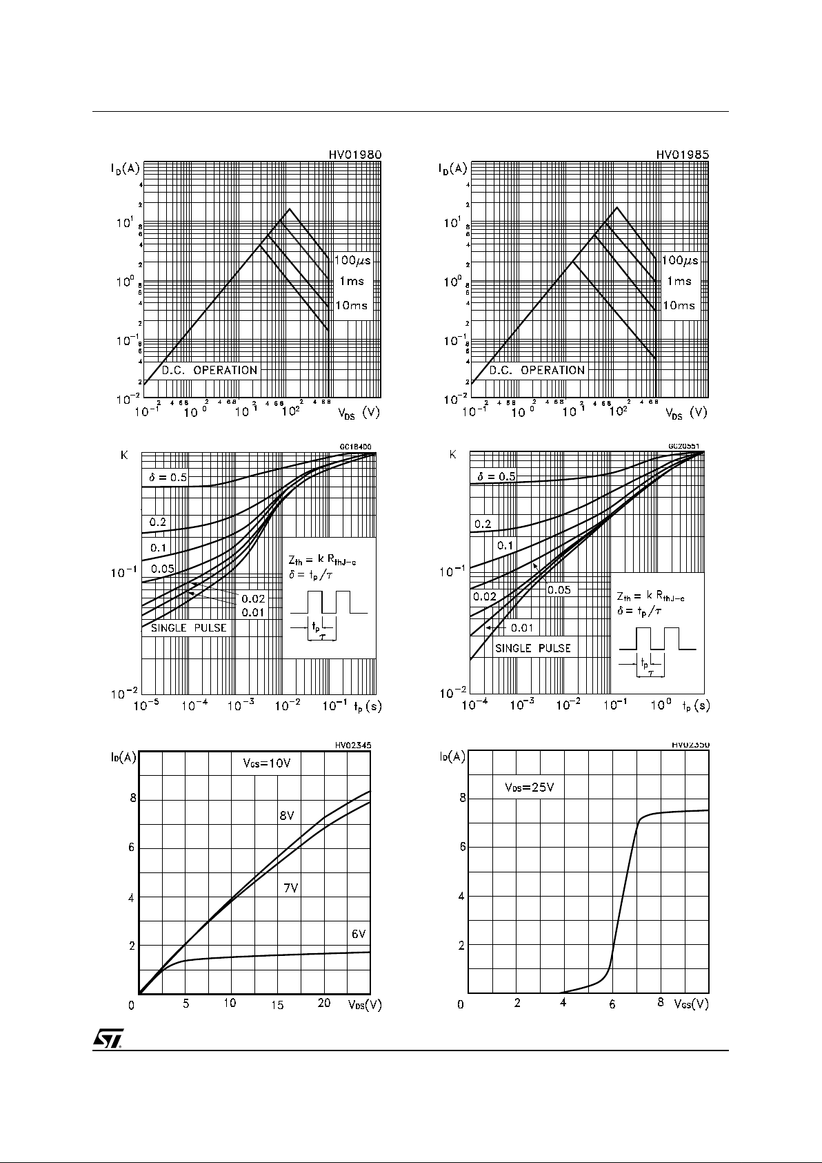
Safe Operating Area For TO-220FPSafe Operating Area For TO-220/D²PAK/I²PA K
Output Characteristics
Thermal Impedance For TO-220/D²PAK/I²PA K
Thermal Impedance For TO-220FP
Transfer Characteristics
 Loading...