

SGS Thomson Microelectronics STP4NB80 Datasheet
STP4NB80
N - CHANNEL 800V - 3Ω - 4A TO-220/TO-220FP
TYPE V
STP4NB80
STP4NB80FP
■ TYPICALR
■ EXTREMELYHIGH dv/dt CAPABILITY
■ 100%AVALANCHETESTED
■ VERYLOW INTRINSIC CAPACITANCES
■ GATECHARGE MINIMIZED
DS(on)
DSS
800 V
800 V
=3Ω
DESCRIPTION
Using the latest high voltage MESH OVERLAY
process, STMicroelectronics has designed an
advanced family of power MOSFETs with
outstanding performances. The new patent
pending strip layout coupled with the Company’s
proprietary edge termination structure, gives the
lowest RDS(on) per area, exceptional avalanche
and dv/dt capabilities and unrivalled gate charge
and switching characteristics.
R
DS(on)
3.3 Ω
3.3 Ω
I
D
4A
4A
STP4NB80FP
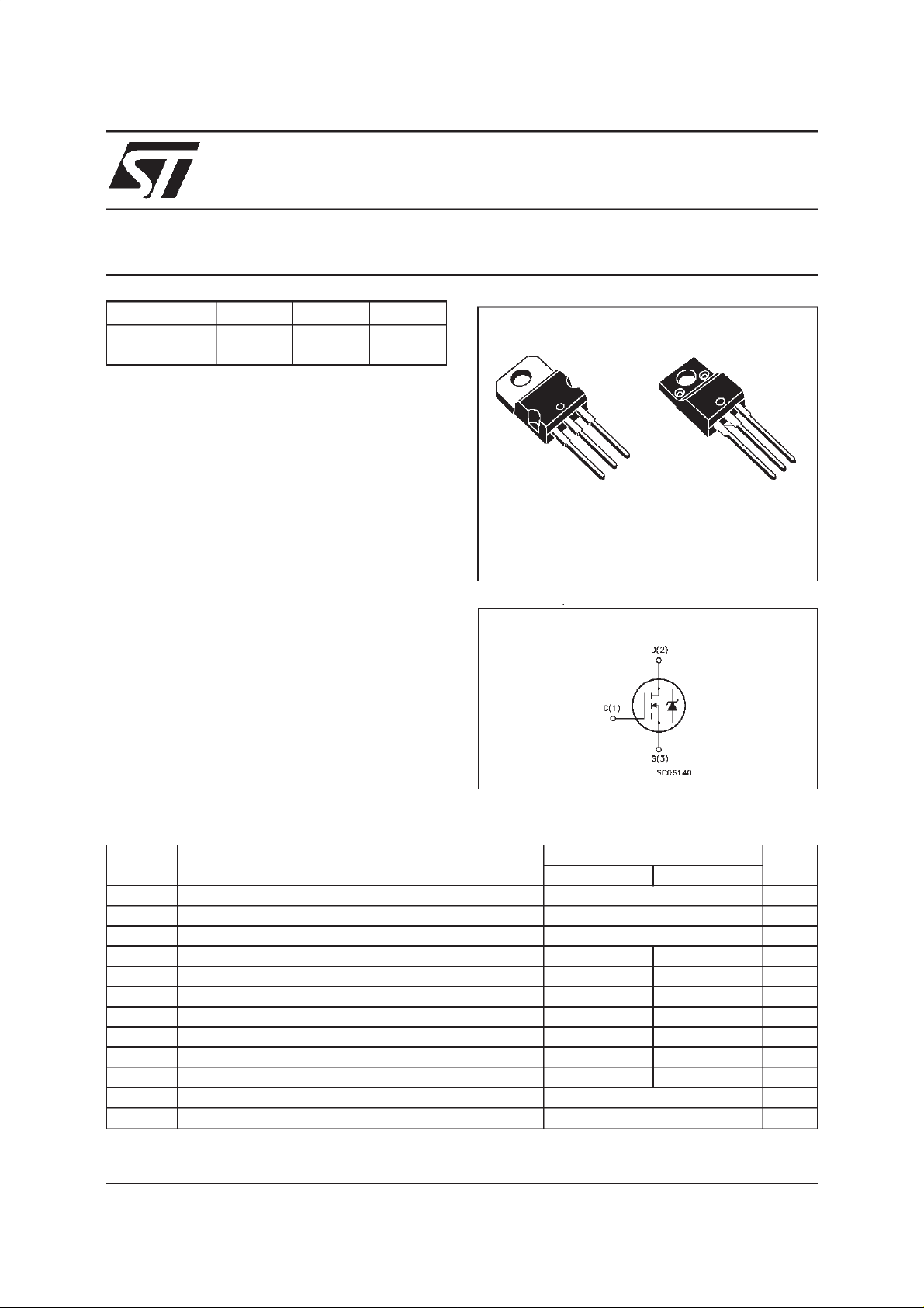
PowerMESH MOSFET
3
2
1
TO-220 TO-220FP
INTERNAL SCHEMATIC DIAGRAM
3
2
1
APPLICATIONS
■ HIGHCURRENT, HIGHSPEEDSWITCHING
■ SWITCHMODE POWER SUPPLIES (SMPS)
■ DC-AC CONVERTERS FOR WELDING
EQUIPMENTANDUNINTERRUPTIBLE
POWERSUPPLIESAND MOTORDRIVE
ABSOLUTE MAXIMUM RATINGS
Symbol Parameter Value Unit
ST P4NB8 0 ST P4NB 80FP
V
V
V
I
DM
P
dv/dt(
V
T
(•) Pulse widthlimited by safe operating area (1)ISD≤4 A, di/dt ≤ 200 A/µs,VDD≤ V
(*)
Limited only by maximum temperature allowed
March 2000
Dra in- sour c e Volt age (VGS= 0) 800 V
DS
Dra in- gat e Voltage (RGS=20kΩ) 800 V
DGR
Gat e-source Voltage
GS
Dra in Cu rr ent (contin uous ) a t Tc=25oC 4 4(*) A
I
D
Dra in Cu rr ent (contin uous ) a t Tc=100oC 2.4 2.4(* ) A
I
D
30 V
±
(•) Dra in Cu rr ent (pulsed) 16 16 A
Tot al Dissipat ion at Tc=25oC 100 35 W
tot
Der ati ng Fact or 0.8 0.28 W/
1) Peak Diode Recov ery volt age sl ope 4.5 4.5 V/ns
Insulation Withstand Voltage (DC) 20 00 V
ISO
St orage Temperat ure -65 to 150
stg
Max. Operating Junct ion Temper atur e 150
T
j
(BR)DSS
,Tj≤T
JMAX
o
C
o
C
o
C
1/9
STP4NB80/FP
THERMAL DATA
TO-220 TO220-FP
R
thj-case
R
thj-amb
R
thc-sink
T
AVALANCHE CHARACTERISTICS
Symbol Parameter Max V alue Unit
I
AR
E
Ther mal Resistanc e Junct ion-case Ma x 1.25 3 . 6
Ther mal Resistanc e Junct ion-ambient Max
Ther mal Resistanc e Case-sink Ty p
Maximum Lead T empera tur e F or S o ldering Purpos e
l
Avalanche Current, Repetitive or Not-Repetitive
(pulse width limited by T
Single Pul se Avalanc he Ener gy
AS
(starting T
=25oC, ID=IAR,VDD=50V)
j
max)
j
62.5
0.5
300
4A
230 mJ
o
C/W
o
C/W
o
C/W
o
C
ELECTRICAL CHARACTERISTICS
=25oC unless otherwisespecified)
(T
case
OFF
Symbol Parameter Test Conditions Min. Typ. Max. Unit
V
(BR)DSS
Drain-source
ID=250µAVGS= 0 800 V
Break dow n Vo lt age
I
DSS
I
GSS
Zero Gate Voltage
Drain Curre nt (V
GS
Gat e- bod y Leakag e
Current (V
DS
=0)
=0)
V
=MaxRating
DS
=MaxRating Tc=125oC
V
DS
V
=± 30 V
GS
1
50
100 nA
±
ON (∗)
Symbol Parameter Test Conditions Min. Typ. Max. Unit
V
GS(th)
R
DS(on)
Gate Threshold Voltage VDS=VGSID= 250µA 345V
Sta t ic Drain-s our c e On
VGS=10V ID=2A 3 3.3
Resistance
I
D(on)
On State Drain Current VDS>I
D(on)xRDS(on)max
4A
VGS=10V
DYNAMIC
Symbol Parameter Test Conditions Min. Typ. Max. Unit
g
(∗)Forward
fs
Tr ansc on duc tance
C
C
C
Input Capaci t ance
iss
Out put Capac itance
oss
Reverse Transfer
rss
Capacit a nc e
VDS>I
D(on)xRDS(on)maxID
=2A 1.5 2.9 S
VDS=25V f=1MHz VGS= 0 700
95
9
920
126
12
µA
µA
Ω
pF
pF
pF
2/9
STP4NB80/FP
ELECTRICAL CHARACTERISTICS
(continued)
SWITCHING ON
Symbol Parameter Test Conditions Min. Typ. Max. Unit
t
d(on)
Q
Q
Q
t
Turn-on Time
Rise Time
r
Tot al Gate Charge
g
Gat e- Source Charge
gs
Gate-Drain Charge
gd
VDD=400V ID=2A
R
=4.7
G
Ω
VGS=10V
14
8
VDD= 640 V ID=4A VGS=10V 21
7
9
20
12
29 nC
SWITCHING OFF
Symbol Parameter Test Conditions Min. Typ. Max. Unit
t
r(Voff)
t
t
Off-voltage Rise T im e
Fall T ime
f
Cross-over Tim e
c
VDD= 640V ID=4A
=4.7 Ω VGS=10V
R
G
12
16
17
9
13
22
SOURCEDRAINDIODE
Symbol Parameter Test Conditions Min. Typ. Max. Unit
I
SD
I
SDM
V
SD
t
Q
I
RRM
(∗) Pulsed:Pulse duration= 300µs, duty cycle 1.5%
(•) Pulse width limited by safe operatingarea
Source-drain Current
(•)
Source-drain Current
4
16
(pulsed)
(∗)ForwardOnVoltage ISD=4 A VGS=0 1.6 V
Reverse Recovery
rr
Time
Reverse Recovery
rr
ISD=4A di/dt=100A/µs
= 100 V Tj=150oC
V
DD
600
3.3
Charge
Reverse Recovery
11
Current
ns
ns
nC
nC
ns
ns
ns
A
A
ns
µ
A
C
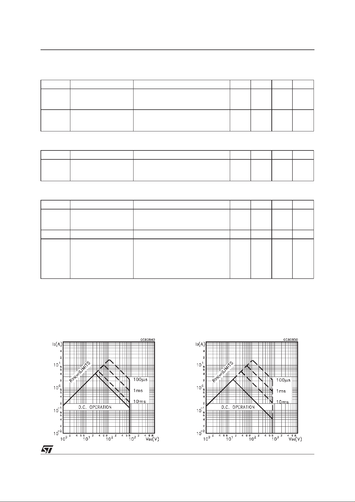
SafeOperating Area for TO-220 SafeOperating Area for TO-220FP
3/9
 Loading...