

STP45NF06
N-CHANNEL 60V - 0.022Ω - 38A TO-220
STripFET™ POWER MOSFET
PRELIMINARY DATA
TYPE V
DSS
STP45NF06 60V <0.028
■ TYPICAL R
■ EXCEPTIONAL dv/d t CAPABILITY
(on) = 0.022Ω
DS
R
DS(on)
I
D
Ω
38A
DESCRIPTION
This Power Mosfet is the latest development of
STMicroelectronics unique “Single Feature
Size
™” strip-based process. The re sulting tran-
sistor shows extremely high packing density for
low on-resistance, rugged avalance characteristics and less critical alignment steps therefore a remarkable manufacturing reproducibility.
APPLICATIONS
■ HIGH-EFFICIENCY DC-DC CONVERTERS
■ SOLENOID AND RELAY DRIVERS
■ MOTOR CONTROL, AUDIO AMPLIFIERS
■ DC-DC & DC-AC CONVERTERS
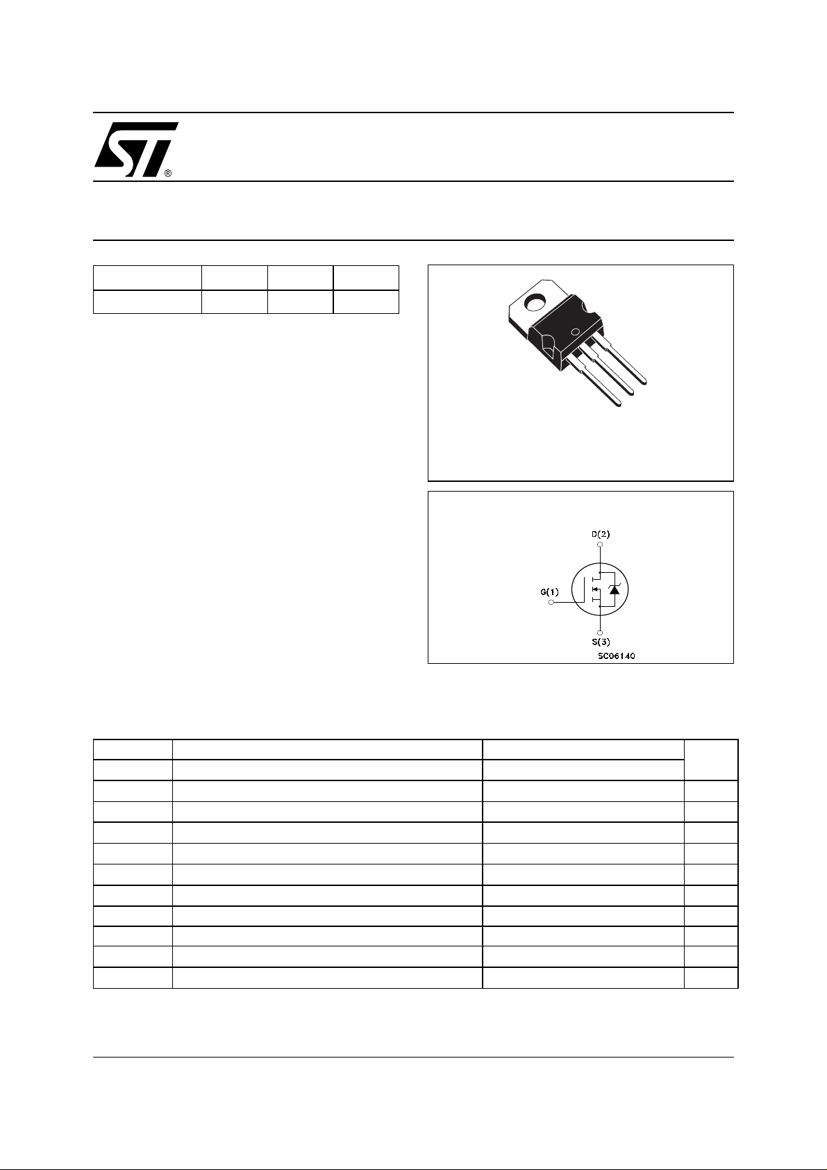
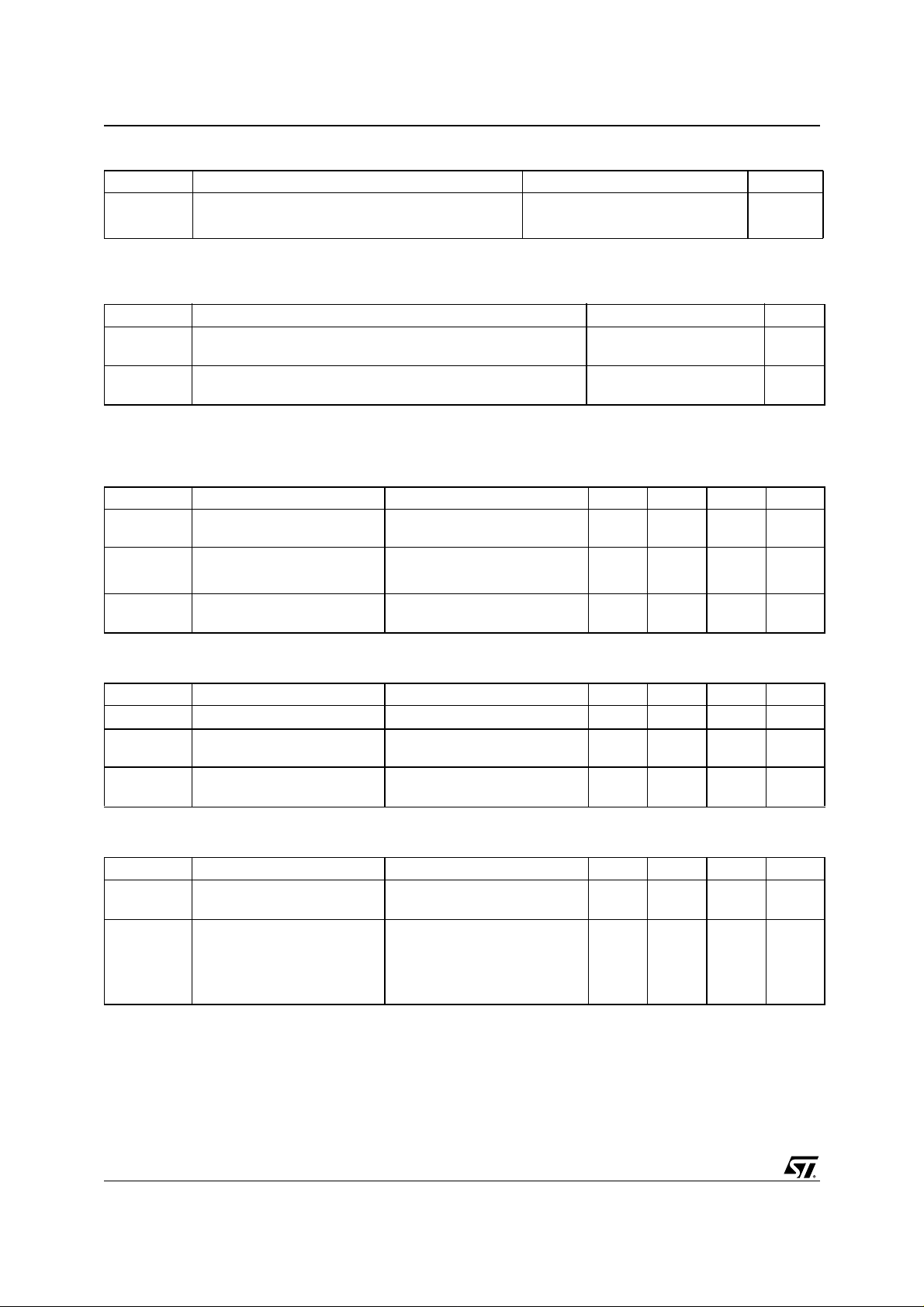
3
2
1
TO-220
INTERNAL SCHEMATIC DIAGRAM
ABSOLUTE MAXIMUM RATINGS
Symbol Parameter Value Unit
V
DS
V
DGR
V
GS
I
D
I
D
I
DM
P
TOT
dv/dt (1) Peak Diode Recovery voltage slope 7 V/ns
T
stg
T
j
(●) Pulse width limited by safe operating area
November 2000
This is preliminary information on a new product now in development or undergoing evaluation. Details are subject to change without notice.
Drain-source Voltage (VGS = 0)
Drain-gate Voltage (RGS = 20 kΩ)
60 V
60 V
Gate- source Voltage ±20 V
Drain Current (continuos) at TC = 25°C
Drain Current (continuos) at TC = 100°C
(●)
Drain Current (pulsed) 152 A
Total Dissipation at TC = 25°C
38 A
26 A
80 W
Derating Factor 0.53 W/°C
Storage Temperature –65 to 175 °C
Max. Operating Junction Temperature 175 °C
(1) ISD ≤38A, di/dt ≤300A/µs, VDD ≤ V
(BR)DSS
, Tj ≤ T
JMAX.
1/6
STP45NF06
THERMA L D ATA
Rthj-case Thermal Resistance Junction-case Max 1.87 °C/W
Rthj-amb Thermal Resistance Junction-ambient Max 62.5 °C/W
T
l
AVALANCHE CHARACTERISTICS
Symbol Parameter Max Value Unit
I
AR
E
AS
ELECTRICAL CHARACTERISTICS (TCASE = 25 °C UNLESS OTHERWISE SPECIFIED)
OFF
Symbol Parameter Test Conditions Min. Typ. Max. Unit
V
(BR)DSS
I
DSS
I
GSS
Maximum Lead Temperature For Soldering Purpose 300 °C
Avalanche Current, Repetitive or Not-Repetitive
(pulse width limited by T
max)
j
Single Pulse Avalanche Energy
(starting T
Drain-source
Breakdown Voltage
Zero Gate Voltage
Drain Current (V
Gate-body Leakage
Current (V
= 25 °C, ID = IAR, VDD = 50 V)
j
= 250 µA, VGS = 0
I
D
= Max Rating
V
DS
= 0)
DS
GS
= 0)
V
= Max Rating, TC = 125 °C
DS
= ±20V
V
GS
60 V
38 A
135 mJ
1µA
10 µA
±100 nA
ON
(1)
Symbol Parameter Test Conditions Min. Typ. Max. Unit
V
V
GS(th)
R
DS(on)
I
D(on)
Gate Threshold Voltage
Static Drain-source On
Resistance
On State Drain Current
= VGS, ID = 250µA
DS
= 10 V, ID = 19 A
V
GS
V
> I
D(on)
x R
DS
VGS=10V
DS(on)max,
234V
0.022 0.028
45 A
DYNAMIC
Symbol Parameter Test Conditions Min. Typ. Max. Unit
> I
V
(1)
g
fs
C
iss
C
oss
C
rss
Forward Transconductance
Input Capacitance
Output Capacitance 215 pF
Reverse Transfer
Capacitance
I
D
V
DS
=19 A
DS
x R
D(on)
DS(on)max,
= 25V, f = 1 MHz, VGS = 0
24 S
1730 pF
63 pF
Ω
2/6
 Loading...