


SGS Thomson Microelectronics STP45NE06LFP, STP45NE06L Datasheet
STP45NE06L
®
N - CHANNEL 60V - 0.022Ω - 45A - TO-220/TO-220FP
TYPE V
STP45NE06L
STP45NE06LFP
■
TYPICAL R
■
EXCEPTIONAL dv/dt CAPABILITY
■
100% AVALANCHE TESTED
■
LOW GATE CHARGE 100 oC
■
LOW THRESHOLD DRIVE
DS(on)
DSS
60 V
60 V
= 0.022
DESCRIPTION
This Power Mosfet is the latest development of
STMicroelectronics unique "Single Feature
Size" strip-based process. The resulting transistor shows extremely high packing density for low
on-resistance, rugged avalance characteristics
and less critical alignment steps therefore a remarkable manufacturing reproducibility.
APPLICATIONS
■
HIGH CURRENT, HIGH SPEED SWITCH ING
■
SOLENOID AND RELAY DRIVERS
■
MOTOR CONTROL, AUDIO AMPLIFIERS
■
DC-DC & DC-AC CONVERTERS
R
DS(on)
< 0.028 Ω
< 0.028 Ω
Ω
I
D
45 A
25 A
STP45NE06LFP
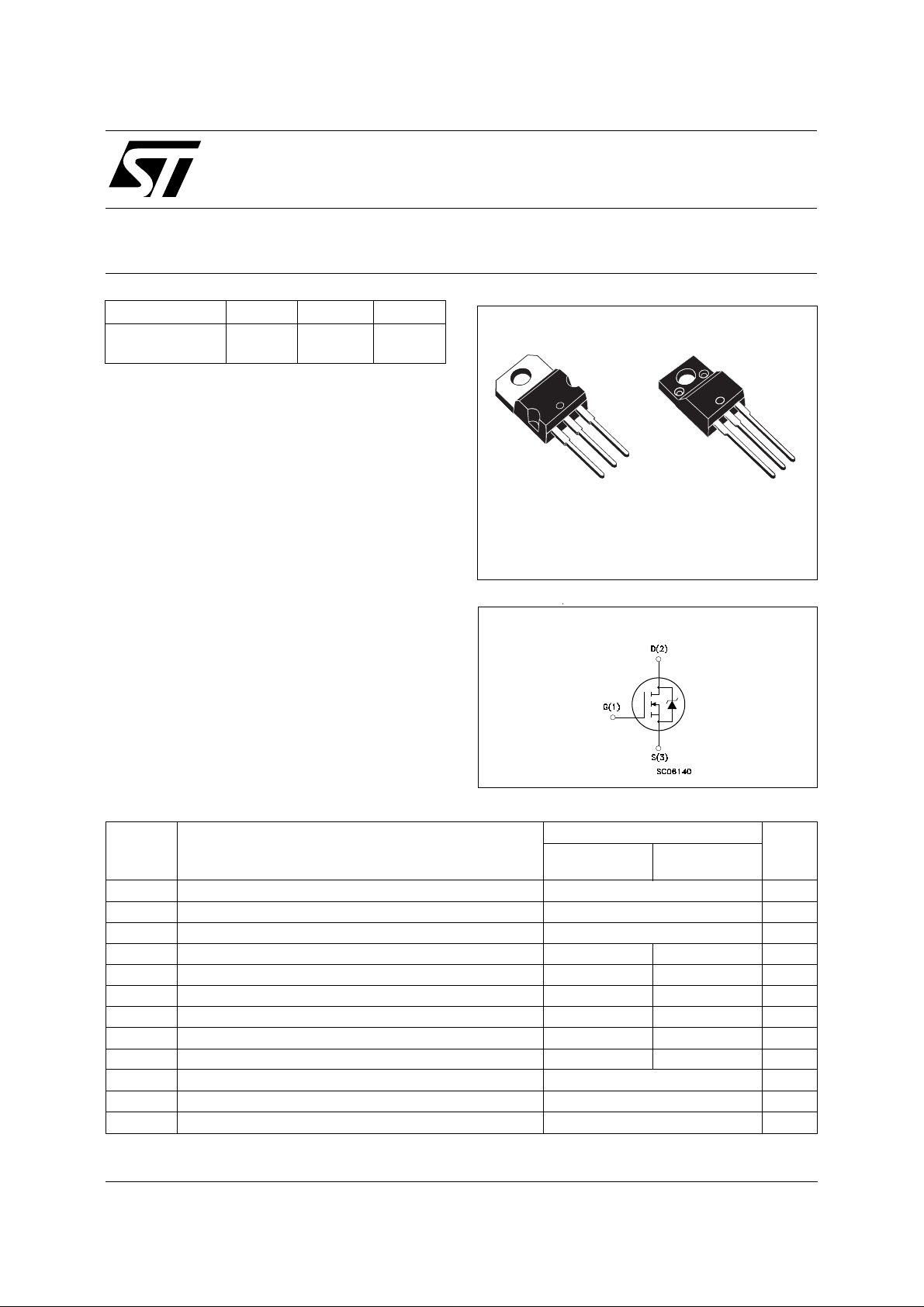
STripFET POWER MOSFET
PRELIMINARY DATA
3
2
1
TO-220 TO-220FP
INTERNAL SCHEMATIC DIAGRAM
3
2
1
ABSOLUTE MAXIMUM RATINGS
Symbol Parameter Value Unit
STP45NE06L STP45NE06LFP
V
V
V
I
DM
P
V
dv/dt Peak Diode Recovery voltage slope 7 V/ns
T
(•) Pulse width limited by safe operating area (1) ISD ≤ 45 A, di/dt ≤ 300 A/µs, VDD ≤ V
June 1999
Drain-source Voltage (VGS = 0) 60 V
DS
Drain- gate Voltage (RGS = 20 kΩ)
DGR
Gate-source Voltage ± 20 V
GS
Drain Current (continuous) at Tc = 25 oC4525A
I
D
I
Drain Current (continuous) at Tc = 100 oC 31 17.5 A
D
60 V
(•) Drain Current (pulsed) 180 180 A
Total Dissipation at Tc = 25 oC 100 35 W
tot
Derating Factor 0.67 0.23 W/
Insulation Withstand Voltage (DC) 2000 V
ISO
Storage Temperature -65 to 175
stg
Max. Operating Junction Temperature 175
T
j
, Tj ≤ T
(BR)DSS
JMAX
o
C
o
C
o
C
1/6
STP45NE06L/FP
THERMAL DATA
TO-220 TO-220FP
R
thj-case
R
thj-amb
R
thc-sink
T
AVALANCHE CHARACTERIST ICS
Symbol Parameter Max Value Unit
I
AR
E
Thermal Resistance Junction-case Max 1.5 4.28
Thermal Resistance Junction-ambient Max
Thermal Resistance Case-sink Typ
Maximum Lead Temperature For Soldering Purpose
l
Avalanche Current, Repetitive or Not-Repetitive
(pulse width limited by T
Single Pulse Avalanche Energy
AS
(starting T
= 25 oC, ID = IAR, V
j
max)
j
DD
= 25V)
62.5
0.5
300
45 A
150 mJ
o
C/W
o
C/W
o
C/W
o
C
ELECTRICAL CHARACTERISTICS
= 25 oC unless otherwise specified)
(T
case
OFF
Symbol Parameter Test Conditions Min. Typ. Max. Unit
V
(BR)DSS
Drain-source
I
= 250 µA V
D
GS
= 0
60 V
Breakdown Voltage
I
DSS
I
GSS
Zero Gate Voltage
Drain Current (V
GS
Gate-body Leakage
Current (V
DS
= 0)
= 0)
= Max Rating
V
DS
V
= Max Rating Tc = 125 oC
DS
V
= ± 20 V
GS
1
10
± 100 nA
ON (∗)
Symbol Parameter Test Conditions Min. Typ. Max. Unit
V
GS(th)
R
DS(on)
I
D(on)
Gate Threshold Voltage
Static Drain-source On
Resistance
V
= VGS ID = 250 µA
DS
VGS = 5 V ID = 22.5 A
V
= 10 V ID = 22.5 A
GS
On State Drain Current VDS > I
V
= 10 V
GS
D(on)
x R
DS(on)max
1 1.7 2.5 V
0.024
0.022
45 A
0.03
0.028ΩΩ
DYNAMIC
Symbol Parameter Test Conditions Min. Typ. Max. Unit
g
(∗) Forward
fs
Transconductance
C
C
C
Input Capacitance
iss
Output Capacitance
oss
Reverse Transfer
rss
Capacitance
VDS > I
V
DS
x R
D(on)
DS(on)max
= 25 V f = 1 MHz V
ID =22.5 A 15 30 S
90
3600
480
100
= 0 2370
GS
350
µA
µA
pF
pF
pF
2/6