

SGS Thomson Microelectronics STP45N10 Datasheet
STP45N10
®
N - CHANNEL 100V - 0.027Ω - 4 5A - TO-220/TO-22 0FI
TYPE V
STP45N10
STP45N10FI
■ TYPICAL R
■ AVALANCHE RUGGED TECHNOLOGY
■ 100% AVALANCHE TESTED
■ REPETITIVE AVA LANCHE DATA AT 100
■ LOW GATE CHARGE
■ HIGH CURRENT CAPABILITY
o
■ 175
■ APPL ICATIO N ORIEN TED
C OPERATING TEMPERATURE
DS(on)
DSS
100 V
100 V
= 0.027 Ω
CHARACTERIZATION
APPLICATIONS
■ HIGH CURRENT, HIGH SPE ED SWI TCHING
■ SOLENOID AND RELAY DRIV ERS
■ DC-DC & DC-AC CONVE RTE RS
■ AUTOMO T IVE ENV I RONME NT (INJ ECT I ON,
ABS, AIR-BAG, LAMP DRIVERS. Etc.)
R
DS(on)
< 0.035 Ω
< 0.035 Ω
I
D
45 A
24 A
o
C
STP45N10FI
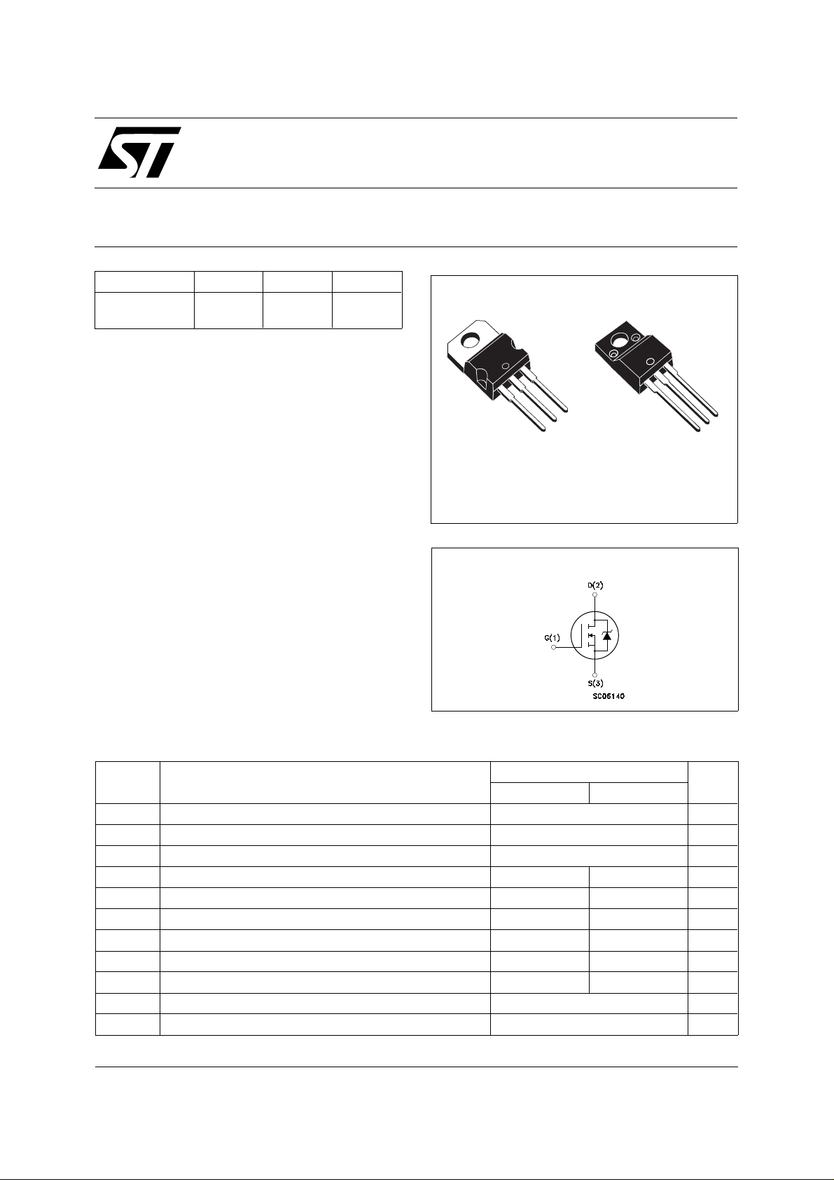
POWER MOS TRANSISTOR
3
2
1
TO-220 ISOWATT220
INTER NAL SCH E M ATI C DIAG RA M
3
2
1
ABSOLUTE MAXIMUM RATINGS
Symbol Parameter Value Unit
STP45N10 STP45N10FI
V
V
V
I
DM
P
V
T
June 1998
Drain-source Voltage (VGS = 0) 100 V
DS
Drain- gate Voltage (RGS = 20 kΩ)
DGR
Gate-source Voltage ± 25 V
GS
I
Drain Current (continuous) at Tc = 25 oC4524A
D
I
Drain Current (continuous) at Tc = 100 oC3217A
D
100 V
(•) Drain Current (pulsed) 180 180 A
Total Dissipation at Tc = 25 oC15045W
tot
Derating Factor 1 0.3 W/oC
Insulation Withstand Voltage (DC) 2 000 V
ISO
Storage Temperature -65 to 175
stg
T
Max. Operating Junction Temperature 175
j
o
o
C
C
1/10
STP45N10/FI
THERMAL DATA
TO220 ISOWATT220
R
thj-case
R
thj-amb
R
thc-sink
T
AVALANCHE CHARACTERI S TICS
Symbol Parameter Max Value Unit
I
AR
E
Thermal Resistance Junction-case Max 1 3.33
Thermal Resistance Junction-ambient Max
Thermal Resistance Case-sink Typ
Maximum Lead Temperature For Soldering Purpose
l
Avalanche Current, Repetitive or Not-Repetitive
(pulse width limited by T
Single Pulse Avalanche Energy
AS
(starting T
= 25 oC, ID = IAR, V
j
ma x, δ < 1%)
j
= 25 V)
DD
62.5
0.5
300
45 A
400 mJ
o
C/W
o
C/W
o
C/W
o
C
ELECTRICAL CHARACTERISTICS (T
= 25 oC unless otherwise specified)
case
OFF
Symbol Parameter Test Conditions Min. Typ. Max. Unit
V
(BR)DSS
Drain-source
I
= 250 µA V
D
GS
= 0
100 V
Breakdown Voltage
I
DSS
I
GSS
Zero Gate Voltage
Drain Current (V
GS
= 0)
Gate-Source Leakage
Current (V
DS
= 0)
= Max Rating
V
DS
V
= Max Rating x 0.8
DS
V
= Max Rating x 0.8 Tc = 125 oC
DS
V
= ± 20 V
GS
10
1
50
± 100 mA
ON (∗)
Symbol Parameter Test Conditions Min. Typ. Max. Unit
V
GS(th)
Gate Threshold
V
= VGS ID = 250 µA
DS
234V
Voltage
R
DS(on)
I
D(on)
Static Drain-source On
Resistance
VGS = 10 V ID = 22.5 A
V
= 10 V ID = 22.5 A Tc = 100oC
GS
On State Drain Current VDS > I
V
= 10 V
GS
D(on)
x R
DS(on)max
0.027 0.035
0.07
45 A
DYNAMIC
Symbol Parameter Test Conditions Min. Typ. Max. Unit
gfs (∗) Forward
Transconductance
C
C
C
Input Capacitance
iss
Output Capacitance
oss
Reverse Transfer
rss
Capacitance
VDS > I
V
DS
x R
D(on)
DS(on)max
= 25 V f = 1 MHz V
ID = 22.5 A 20 40 S
= 0 4100
GS
600
150
5200
800
220
µA
µA
Ω
Ω
pF
pF
pF
2/10
STP45N10/FI
ELECTRICAL CHARACTERISTICS (continued)
SWITCHING O N
Symbol Parameter Test Conditions Min. Typ. Max. Unit
t
d(on)
t
(di/dt)
Q
Q
Q
SWITCHING O F F
Symbol Parameter Test Conditions Min. Typ. Max. Unit
t
r(Voff)
t
SOURCE DRAIN DIO DE
Turn-on Time
Rise Time
r
Turn-on Current Slope V
on
Total Gate Charge
g
Gate-Source Charge
gs
Gate-Drain Charge
gd
Off-voltage Rise Time
Fall Time
t
f
Cross-over Time
c
V
= 50 V ID = 22.5
DD
A
R
= 4.7 Ω VGS = 10 V
G
= 80 V ID = 45 A
DD
= 47 Ω VGS = 10 V
R
G
V
= 80 V ID =45 A V
DD
V
= 80 V ID = 45 A
DD
= 4.7 Ω VGS = 10 V
R
G
GS
25
75
400 A/µs
= 10 V 120
20
50
30
35
65
35
105
170 nC
45
50
95
ns
ns
nC
nC
ns
ns
ns
Symbol Parameter Test Conditions Min. Typ. Max. Unit
45
180
I
SDM
I
SD
Source-drain Current
(•)
Source-drain Current
(pulsed)
V
(∗) Forward On Voltage ISD = 45 A VGS = 0 1.5 V
SD
t
Q
Reverse Recovery
rr
Time
Reverse Recovery
rr
I
= 45 A di/dt = 100 A/µs
SD
V
= 30 V Tj = 150 oC
DD
200
0.14
Charge
I
RRM
Reverse Recovery
14
Current
(∗) Pulsed: Pulse duration = 300 µs, duty cycle 1.5 %
(•) Pulse width limited by safe operating area
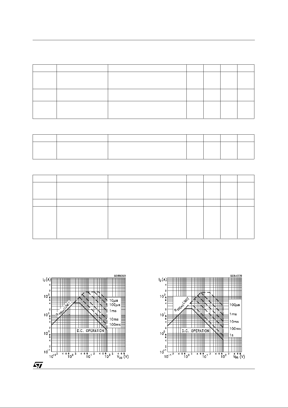
Safe Operating Area for TO-220 Safe Operating Are a for ISOWAT T220
A
A
ns
µC
A
3/10
 Loading...