

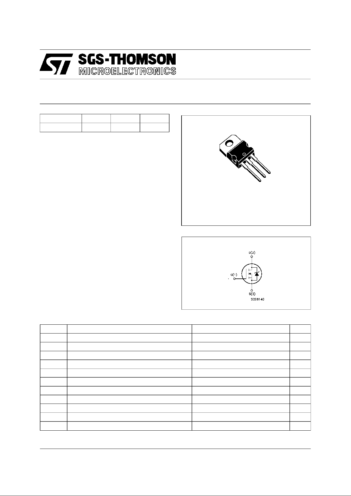
STP38N06
N - CHANNEL ENHANCEMENT MODE
”ULTRA HIGH DENSITY” POWER MOS TRANSISTOR
PRELIMINARY DATA
TYPE V
DSS
STP38N06 60 V < 0.03 Ω 38 A (*)
R
DS(on)
I
D
■ TYPICALR
■ AVALANCHERUGGEDTECHNOLOGY
■ 100% AVALANCHETESTED
■ REPETITIVEAVALANCHEDATAAT 100
■ HIGH CURRENTCAPABILITY
o
■ 175
■ HIGH dV/dt RUGGEDNESS
■ APPLICATIONORIENTED
COPERATINGTEMPERATURE
DS(on)
=0.026 Ω
o
C
CHARACTERIZATION
APPLICATIONS
■ HIGH CURRENT, HIGH SPEEDSWITCHING
■ POWERMOTOR CONTROL
■ DC-DC& DC-AC CONVERTERS
■ SYNCRONOUSRECTIFICATION
3
2
1
TO-220
INTERNAL SCHEMATIC DIAGRAM
ABSOLUTE MAXIMUM RATINGS
Symb o l Parame t er Val u e Uni t
V
V
DGR
V
I
DM
P
dV/dt(
T
(•) Pulse width limited by safe operating area
March 1996
Drain-source Voltage (VGS=0) 60 V
DS
Drain- gate Voltage (RGS=20kΩ)60V
Gate-source Voltage ± 20 V
GS
I
Drain Current (c ont inuo us) a t Tc=25oC38A
D
I
Drain Current (c ont inuo us) a t Tc=100oC26A
D
(•) Drain Current (puls ed) 152 A
Total Dissipat i on at Tc=25oC90W
tot
Derat ing Factor 0.6 W/
1) Peak Diode Recovery voltage slope 7 V/ns
Stora ge Temperature -65 to 175
stg
T
Max. Operat ing Junct i on Temperatu re 175
j
o
o
o
C
C
C
1/11
STP38N06
THERMAL DATA
R
thj-case
R
thj-amb
R
thc-sin k
T
AVALANCHE CHARACTERISTICS
Symb o l Para met er Max V alue Uni t
I
AR
E
E
I
AR
Ther mal Resistance Junct ion-case Max
Ther mal Resistance Junct ion-ambient Max
Ther mal Resistance Case-s i nk Typ
Maximum Lead Tempera t ure For Solder ing Purpo se
l
Avalanche Current , Repet it iv e or Not-Repe t it ive
(pulse width limi t ed by T
Single Pu lse Avalanc he E nerg y
AS
(starti ng T
Repetitive Avalanche Energy
AR
=25oC, ID=IAR,VDD=25V)
j
(pulse width limi t ed by T
max, δ <1%)
j
max, δ <1%)
j
Avalanche Current , Repet it iv e or Not-Repe t it ive
=100oC, p ulse wid t h limited by Tjmax, δ <1%)
(T
c
1.66
62.5
0.5
300
38 A
300 mJ
75 mJ
26 A
o
C/W
o
C/W
o
C/W
o
C
ELECTRICAL CHARACTERISTICS (T
=25oC unlessotherwise specified)
case
OFF
Symbol Parameter Test Condition s Min. Typ. Max. Unit
V
(BR)DSS
Drain-source
ID= 250 µAVGS=0 60 V
Break dow n Voltage
I
I
DSS
GSS
Zero Gate Voltage
Drain Current (V
GS
Gat e- bod y Leaka ge
Current (V
DS
=0)
=0)
=MaxRating
V
DS
V
=MaxRatingx0.8 Tc= 125oC
DS
V
= ± 20 V ± 100 nA
GS
250
1000µAµA
ON (∗)
Symbol Parameter Test Condition s Min. Typ. Max. Unit
V
GS(th )
R
DS(on)
I
D(on)
Gat e Thre shold Volt age VDS=VGSID=250µA234V
St at ic Drain-source On
Resistance
VGS= 10V ID=19A
= 10V ID=19A Tc=100oC
V
GS
On State Drain Current VDS>I
D(on)xRDS(on)max
0.026 0.03
0.06
38 A
VGS=10V
DYNAMIC
Symbol Parameter Test Condition s Min. Typ. Max. Unit
g
(∗)Forward
fs
Tr ansc on ductance
C
C
C
Input Capac it an ce
iss
Out put Capac itance
oss
Reverse Transfer
rss
Capacit a nc e
VDS>I
D(on)xRDS(on)maxID
=19A 14 19 S
VDS=25V f=1MHz VGS= 0 2000
350
80
2800
450
120
Ω
Ω
pF
pF
pF
2/11
STP38N06
ELECTRICAL CHARACTERISTICS (continued)
SWITCHINGON
Symbol Parameter Test Condition s Min. Typ. Max. Unit
t
d(on)
t
r
Turn-on Time
Rise Time
VDD=30V ID=19A
=50 Ω VGS=10V
R
G
(see test cir cuit, figure 3)
(di/dt)
Tur n-on C urr ent Slope VDD=48V ID=38A
on
R
=50 Ω VGS=10V
G
(see test cir cuit, figure 5)
Q
Q
Q
Tot al Gat e Charge
g
Gate-Source Charge
gs
Gat e- Drain Charge
gd
VDD=40V ID=38A VGS=10V 60
SWITCHINGOFF
Symbol Parameter Test Condition s Min. Typ. Max. Unit
t
r(Voff)
t
Off -voltage Rise Time
t
Fall T ime
f
Cross-over Time
c
VDD=48V ID=38A
=50 Ω VGS=10V
R
G
(see test cir cuit, figure 5)
SOURCE DRAIN DIODE
45
28065380
240 A/ µs
80 nC
10
20
65
140
230
85
180
300
ns
ns
nC
nC
ns
ns
ns
Symbol Parameter Test Condition s Min. Typ. Max. Unit
I
I
SDM
SD
Source-drain Current
(•)
Source-drain Current
38
152
(pulsed)
(∗)ForwardOnVoltage ISD=38A VGS=0 1.5 V
V
SD
t
Q
Reverse Recovery
rr
Time
Reverse Recovery
rr
ISD= 38 A di/dt = 10 0 A/µs
=40V Tj= 150oC
V
DD
(see test cir cuit, figure 5)
85
0.3
Charge
I
RRM
Reverse Recovery
7
Current
(∗) Pulsed: Pulse duration =300 µs,duty cycle 1.5 %
(•) Pulse width limited by safe operating area
(
1)I
≤ 20 A, di/dt≤ 300 A/µs, VDD≤ V
SD
(BR)DSS,Tj≤TJMAX
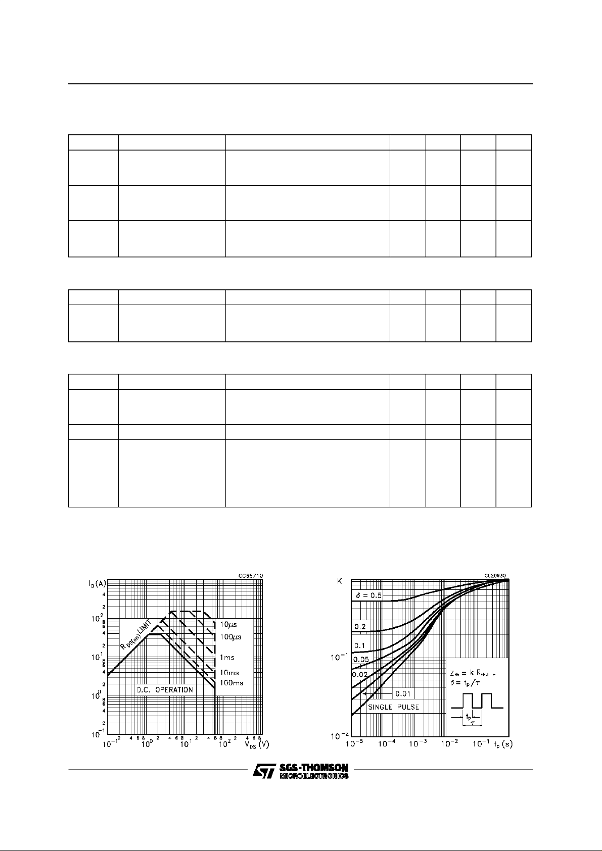
Safe Operating Area ThermalImpedance
A
A
ns
µC
A
3/11
STP38N06
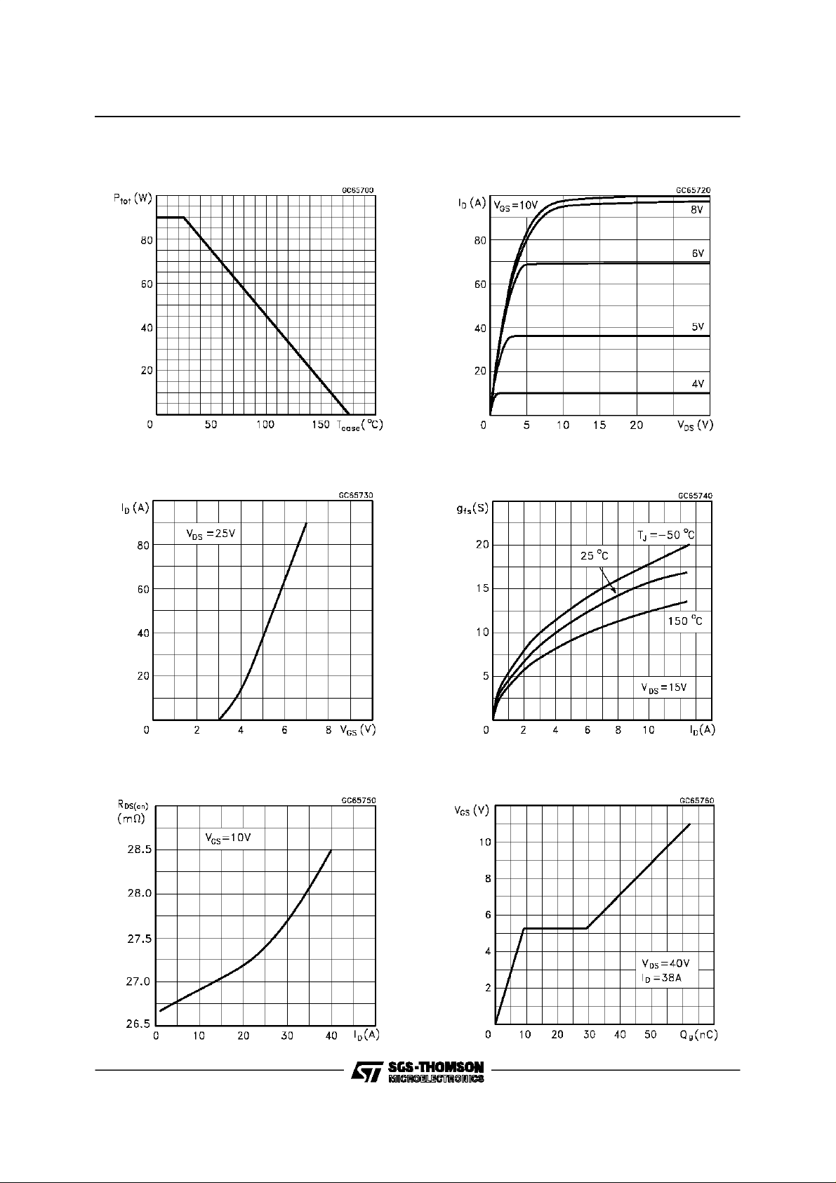
Derating Curve
TransferCharacteristics
OutputCharacteristics
Transconductance
StaticDrain-source On Resistance
4/11
Gate Charge vs Gate-source Voltage
 Loading...