

SGS Thomson Microelectronics STP3020L Datasheet
STP3020L
N - CHANNEL 30V - 0.019Ω - 40A - TO-220
STripFET POWER MOSFET
TYPE V
DSS
R
DS(on)
I
D
ST P3020L 30 V < 0.022 Ω 40 A
■ TYPICALR
■ LOW GATE CHARGE A 100
■ APPLICATIONORIENTED
DS(on)
= 0.019 Ω
o
C
CHARACTERIZATION
DESCRIPTION
This Power Mosfet is the latest development of
STMicroelectronics unique ”Single Feature
Size” strip-based process. The resulting transi-
stor showsextremelyhigh packingdensity forlow
on-resistance, rugged avalance characteristics
and less critical alignment steps therefore a remarkablemanufacturingreproducibility.
APPLICATIONS
■ HIGHCURRENT, HIGH SPEEDSWITCHING
SOLENOIDANDRELAY DRIVERS
■ MOTORCONTROL, AUDIOAMPLIFIERS
■ DC-AC & DC-AC CONVERTERS IN HIGH
PERFORMANCE VRMs
■ AUTOMOTIVE ENVIRONMENT (INJECTION,
ABS, AIR-BAG, LAMPDRIVERS,Etc.)
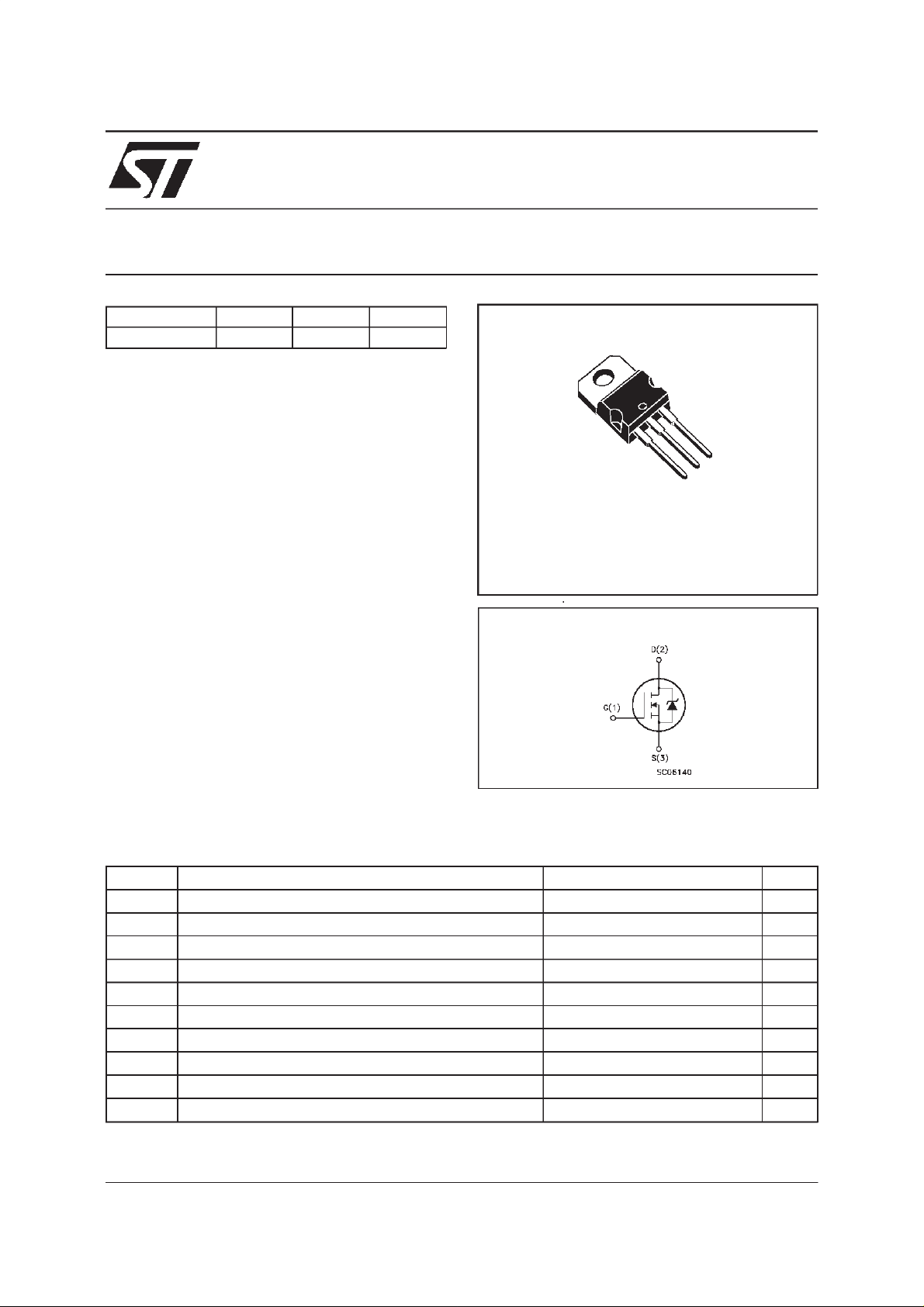
3
2
1
TO-220
INTERNAL SCHEMATIC DIAGRAM
ABSOLUTE MAXIMUM RATINGS
Symb o l Parameter Val u e Uni t
V
V
V
I
DM
P
T
(•) Pulse width limited by safe operating area
March 1999
Drain-sourc e V o lt age (VGS=0) 30 V
DS
Drain- ga t e Voltage (RGS=20kΩ)30V
DGR
Gate-s ource Volt age
GS
I
Drain Cur rent (c ont i nuous) at Tc=25oC40A
D
I
Drain Cur rent (c ont i nuous) at Tc= 100oC28A
D
20 V
±
(•) Drain Current (pulsed) 160 A
Total Dissipation at Tc=25oC80W
tot
Derating Factor 0.53 W/
St orage T em p erat ure -65 to 175
stg
T
Max. Operating Junct ion Tem p er at u re 175
j
o
C
o
C
o
C
1/8
STP3020L
THERMAL DATA
R
thj-case
Rthj-amb
R
thc-sink
T
Ther mal Resistanc e Junct ion-case Max
Ther mal Resistanc e Junct ion-ambient Max
Ther mal Resistanc e Case-sink Ty p
Maximum L ead Tem pe ra t ure For Soldering Purpose
l
1.875
62.5
0.5
300
o
C/W
oC/W
o
C/W
o
C
ELECTRICAL CHARACTERISTICS
=25oC unless otherwisespecified)
(T
case
OFF
Symbol Parameter Test Conditions Min. Typ. M ax. Unit
V
(BR)DSS
Drain-source
ID=250µAVGS=0 30 V
Break dow n Vo lt age
I
DSS
I
GSS
Zero Gate Voltage
Drain Curre nt (V
GS
Gat e- bod y Leakage
Current (V
DS
=0)
=0)
V
=MaxRating
DS
=MaxRating Tc=125oC
V
DS
V
= ± 20 V ± 100 nA
GS
1
10
ON (∗)
Symbol Parameter Test Conditions Min. Typ. M ax. Unit
V
GS(th)
R
DS(on)
I
D(on)
Gate Threshold Voltage VDS=VGSID= 250 µ A12.5V
Sta t ic Drain-s ource On
Resistance
VGS=10V ID=20A
=5V ID=20A
V
GS
On State Drain Current VDS>I
D(on)xRDS(on)max
0.019
0.033
40 A
0.022
0.038ΩΩ
VGS=10V
DYNAMIC
Symbol Parameter Test Conditions Min. Typ. M ax. Unit
g
(∗)Forward
fs
Tr ansc on duc tance
C
C
C
Input Capaci t ance
iss
Out put Capac it anc e
oss
Reverse Transfer
rss
Capacit a nc e
VDS>I
D(on)xRDS(on)maxID
=20 A 5 20 S
VDS=25V f=1MHz VGS= 0 1270
350
115
µ
µA
pF
pF
pF
A
2/8
STP3020L
ELECTRICAL CHARACTERISTICS
(continued)
SWITCHING ON
Symbol Parameter Test Conditions Min. Typ. M ax. Unit
t
d(on)
Tur n-on Delay Time
Rise Time
t
r
VDD=15V ID=19A
R
=4.7
G
Ω
VGS=4.5V
28
220
(Resis t iv e Load, see fig. 3)
Q
Q
Q
Tot al Gate Char ge
g
Gat e- Source Charge
gs
Gate-Drain Charge
gd
VDD=24V ID=38A VGS=5V 21
9
11
29 nC
SWITCHING OFF
Symbol Parameter Test Conditions Min. Typ. M ax. Unit
t
d(off)
Tur n-of f Dela y Tim e
t
Fall T ime
f
VDD=15V ID=19A
=4.7 Ω VGS=4.5V
R
G
45
35
(Resis t iv e Load, see fig. 3)
t
r(Voff)
t
t
Off-voltage Rise Time
Fall T ime
f
Cross-over Tim e
c
VDD=24V ID=38A
=4.7 Ω VGS=4.5V
R
G
(Indu ct iv e Load, see fig. 5)
30
85
125
SOURCEDRAINDIODE
Symbol Parameter Test Conditions Min. Typ. M ax. Unit
I
SDM
V
I
SD
Q
I
RRM
SD
t
Source-drain Current
(•)
Source-drain Current
40
160
(pulsed)
(∗)ForwardOnVoltage ISD=40A VGS=0 1.5 V
Reverse Recovery
rr
Time
Reverse Recovery
rr
ISD= 38 A di/dt = 100 A/µs
=15V Tj=150oC
V
DD
(see test circuit, fig. 5)
45
60
Charge
Reverse Recovery
2.5
Current
ns
ns
nC
nC
ns
ns
ns
ns
ns
A
A
ns
nC
A
(∗) Pulsed:Pulse duration= 300µs, duty cycle 1.5%
(•) Pulse width limited by safeoperating area
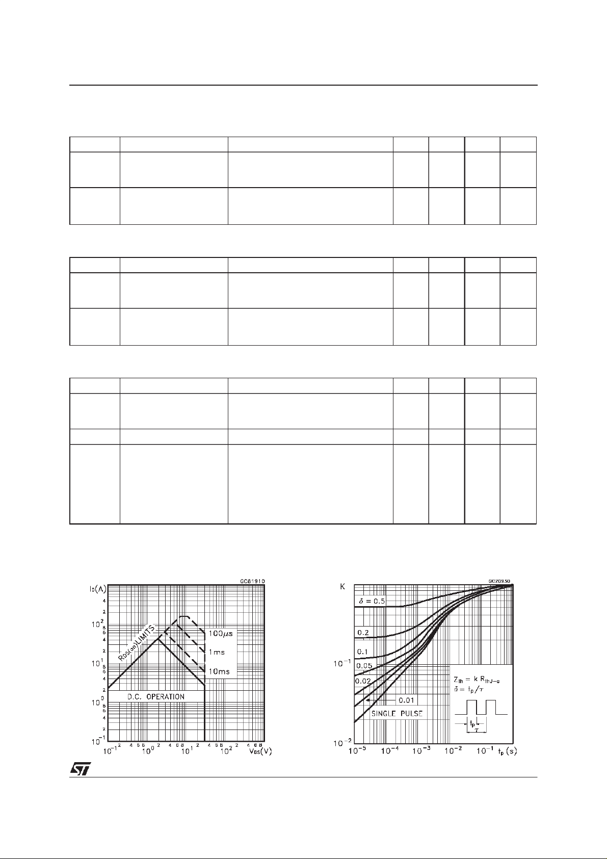
SafeOperating Area ThermalImpedance
3/8
 Loading...