

STB3015L
®
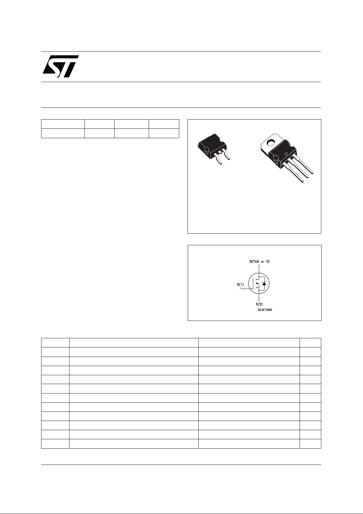
N - CHANNEL 30V - 0.013 Ω - 40A - D2PAK/TO-220
TYPE V
DSS
STB3015L 30 V < 0.0155 Ω 40 A
■ TYPICAL R
■ EXCEPTI ON AL dv/dt CAP AB ILI TY
■ LOW GATE CHARG E A 1 00
■ APPLICATION ORIENTED
DS(on)
= 0.013 Ω
CHARACTERIZATION
■ FOR THROUGH- HOLE VERSIO N
CONTACT SALES OFFICE
DESCRIPTION
This Power MOSFET is the latest development of
STMicroelectronics unique " Single Feature
Size " strip-based process. The resulting transistor shows extremely high packing density for
low on-resistance, rugged avalanche characteristics and less critical alignment steps therefore
a remarkable manufacturing reproducibility.
R
DS(on)
o
C
I
D
STP3015L
STripFET POWER MOSFET
PRELIMINARY DATA
3
1
D2PAK
TO-263
(Suffix "T4")
TO-220
INTER NAL SCH E M ATI C DIAG RA M
3
2
1
APPLICATIONS
■ HIGH CURRENT, HIGH SPE ED SWI TCHING
SOLENOID AND RELA Y DRIVE RS
■ MOTOR CONT RO L, AUDIO AM PLIFI ER S
■ DC-DC & DC-AC CONVERT E RS IN HIGH
PERFORM A NCE VR Ms
■ AUTOMO TIV E ENV IRO NME NT (INJ ECT IO N,
ABS, AIR-BAG, LAMPDRIVERS, Etc.)
ABSOLUTE MAXIMUM RATINGS
Symbol Parameter Value Unit
V
V
V
I
DM
P
dv/dt(
T
(•) Pulse width limited by safe operating area (1) ISD ≤ 40 A, di/dt ≤ 200 A/µs, VDD ≤ V
July 1998
Drain-source Voltage (VGS = 0) 30 V
DS
Drain- gate Voltage (RGS = 20 kΩ)
DGR
Gate-source Voltage ± 20 V
GS
I
Drain Current (continuous) at Tc = 25 oC40A
D
I
Drain Current (continuous) at Tc = 100 oC28A
D
30 V
(•) Drain Current (pulsed) 160 A
Total Dissipation at Tc = 25 oC80W
tot
Derating Factor 0.53 W/oC
1) Peak Diode Recovery voltage slope 7 V/ns
Storage Temperature -65 to 175
stg
T
Max. Operating Junction Temperature 175
j
, Tj ≤ T
(BR)DSS
JMAX
o
C
o
C
1/5
STB3015L
THERMAL DATA
R
thj-case
R
thj-amb
R
thc-si n k
T
Thermal Resistance Junction-case Max
Thermal Resistance Junction-ambient Max
Thermal Resistance Case-sink Typ
Maximum Lead Temperature For Soldering Purpose
l
AVALANCHE CHARACTERI S TICS
Symbol Parameter Max Value Unit
I
AR
E
Avalanche Current, Repetitive or Not-Repetitive
(pulse width limited by T
Single Pulse Avalanche Energy
AS
(starting T
= 25 oC, ID = IAR, V
j
ma x)
j
DD
= 15 V)
1.88
62.5
0.5
300
40 A
200 mJ
o
C/W
o
C/W
o
C/W
o
C
ELECTRICAL CHARACTERISTICS (T
= 25 oC unless otherwise specified)
case
OFF
Symbol Parameter Test Conditions Min. Typ. Max. Unit
V
(BR)DSS
Drain-source
I
= 250 µA V
D
GS
= 0
30 V
Breakdown Voltage
I
DSS
I
GSS
Zero Gate Voltage
Drain Current (V
GS
Gate-body Leakage
Current (V
DS
= 0)
= 0)
= Max Rating
V
DS
V
= Max Rating Tc = 125 oC
DS
V
= ± 20 V
GS
1
10
± 100 nA
ON (∗)
Symbol Parameter Test Conditions Min. Typ. Max. Unit
V
GS(th)
Gate Threshold
V
= VGS ID = 250 µA
DS
1 2.5 V
Voltage
R
DS(on)
I
D(on)
Static Drain-source On
Resistance
V
= 10 V ID = 20 A
GS
V
= 5 V ID = 20 A
GS
On State Drain Current VDS > I
V
= 10 V
GS
D(on)
x R
DS(on)max
0.013 0.0155
0.022ΩΩ
40 A
DYNAMIC
Symbol Parameter Test Conditions Min. Typ. Max. Unit
g
(∗) Forward
fs
Transconductance
C
C
C
Input Capacitance
iss
Output Capacitance
oss
Reverse Transfer
rss
Capacitance
VDS > I
V
DS
x R
D(on)
DS(on)max
= 25 V f = 1 MHz V
ID =20 A 15 20 S
= 0 2500
GS
1200
400
µA
µA
pF
pF
pF
2/5
 Loading...