

SGS Thomson Microelectronics STP24NF10 Datasheet
N - CHANNEL 100V - 0.07Ω - 24A TO-220
LOW GATE CHARGE STripFET POWER MOSFET
TYPE V
DSS
ST P24NF10 100 V < 0.0 77 Ω 24 A
■ TYPICALR
■ EXCEPTIONALdv/dtCAPABILITY
■ 100%AVALANCHETESTED
■ APPLICATIONORIENTED
DS(on)
= 0.07 Ω
CHARACTERIZATION
R
DS(on)
I
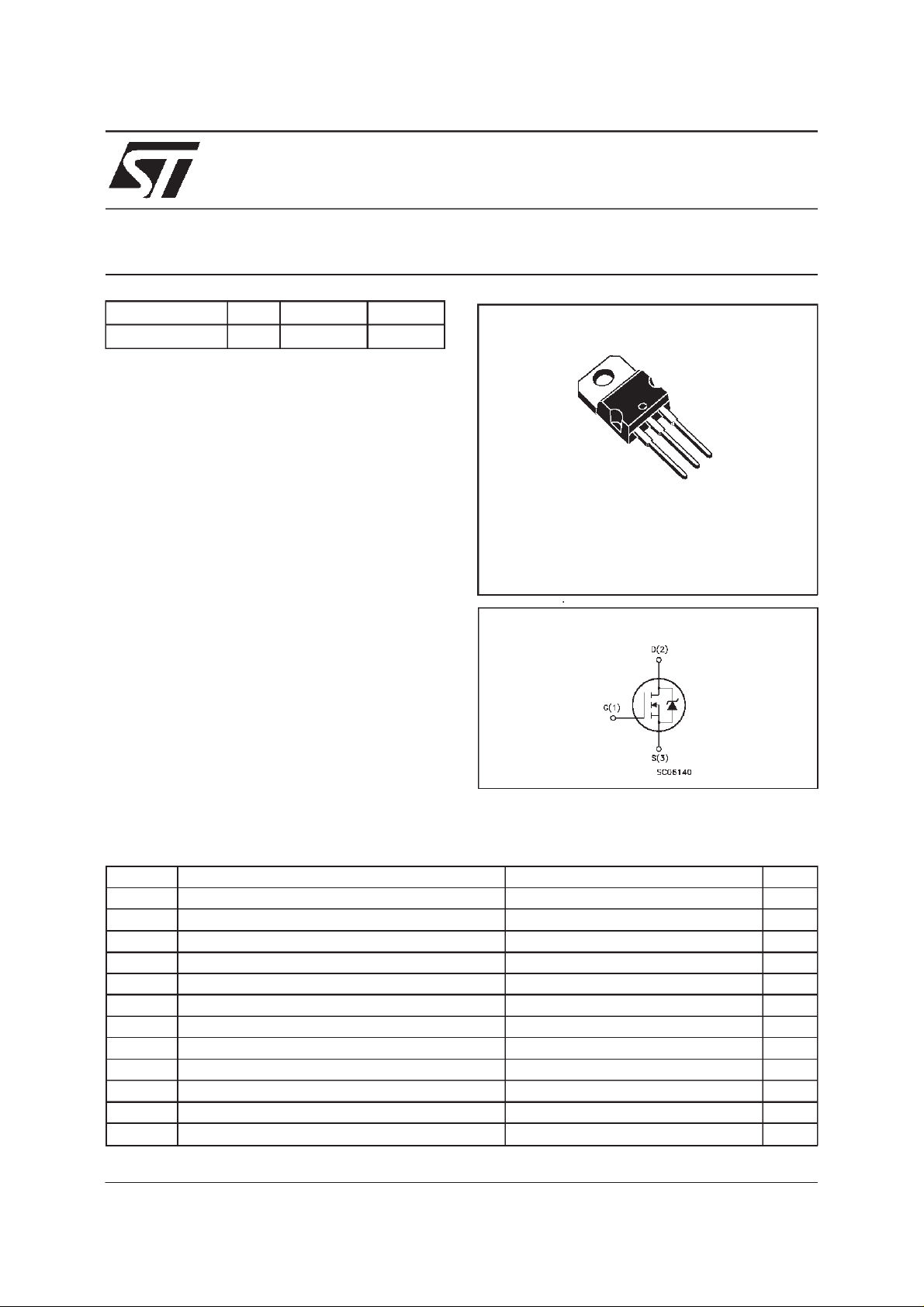
STP24NF10
PRELIMINARY DATA
D
DESCRIPTION
This MOSFET series realized with
3
2
1
STMicroelectronicsunique STripFET process has
specifically been designed to minimize input
TO-220
capacitance and gate charge. It is therefore
suitable as primary switch in advanced
high-efficiency, high-frequency isolated DC-DC
converters for Telecom and Computer
applications. It is also intended for any
applicationswith low gate drive requirements.
INTERNAL SCHEMATIC DIAGRAM
APPLICATIONS
■ HIGH-EFFICIENCYDC-DC CONVERTERS
■ UPSAND MOTORCONTROL
ABSOLUTE MAXIMUM RATINGS
Symbol Parameter Value Uni t
V
V
V
I
DM
P
dv/ dt (
E
AS
T
(•) Pulse width limitedby safe operating area (2) starting Tj
April 2000
Dra in- sour c e Vol ta ge (VGS= 0) 100 V
DS
Drain- gate Voltage (RGS=20kΩ) 100 V
DGR
Gate-s ource Voltage ± 20 V
GS
Dra in Current ( cont inuous) at Tc=25oC24A
I
D
Dra in Current ( cont inuous) at Tc= 100oC15A
I
D
(•) Dra in Current ( pulsed) 96 A
Tot al Dissipatio n a t Tc=25oC80W
tot
Der ati ng Fact or 0.53 W/
1 ) Peak Diode Reco ve ry volta ge slope 9 V/ns
(2) Single Pu lse Avalanche Energy 75 m J
St orage T e m pe ra tur e -65 to 175
stg
Max. Operat ing Junct ion Temperat ur e 175
T
j
=25oC, ID=24A, VDD= 50V (1) ISD≤ 24 A, di/dt ≤ 300A/µs, VDD≤ V
(BR)DSS,Tj≤TJMA
o
C
o
C
o
C
1/6
STP24NF10
THERMAL DATA
R
thj-case
R
thj-amb
T
Ther mal Resistanc e Junct ion-case Max
Ther mal Resistanc e Junct ion-ambient Max
Maximum Lead Temperat ur e For So lder ing Purp ose
l
1.87
62.5
300
o
C/W
o
C/W
o
C
ELECTRICAL CHARACTERISTICS
=25oC unless otherwisespecified)
(T
case
OFF
Symbol Parameter Test Conditions Min. Typ. Max. Unit
V
(BR)DSS
Drain-source
ID=250µAVGS= 0 100 V
Break dow n Voltage
I
DSS
I
GSS
Zero Gate Voltage
Drain Current ( V
GS
Gat e- bod y L eak ag e
Current (V
DS
=0)
=0)
V
=MaxRating
DS
=MaxRating Tc=125oC
V
DS
V
= ± 20 V ± 100 nA
GS
1
10
ON(∗)
Symbol Parameter Test Conditions Min. Typ. Max. Unit
V
GS(th)
R
DS(on)
Gate Threshold Voltage VDS=VGSID= 250 µ A 234V
Sta t ic Drain-sourc e On
VGS=10V ID= 12 A 0.07 0. 07 7 Ω
Resistance
I
D(on)
On State Drain Current VDS>I
D(on)xRDS(on)max
24 A
VGS=10V
DYNAMIC
Symbol Parameter Test Conditions Min. Typ. Max. Unit
g
(∗)Forward
fs
Tr ansc on duc tance
C
C
C
Input C apacitance
iss
Out put Capacitance
oss
Reverse Tr ansfer
rss
Capacit a nc e
VDS>I
D(on)xRDS(on)maxID
=12 A 20 S
VDS=25V f=1MHz VGS= 0 870
125
52
µA
µ
pF
pF
pF
A
2/6
 Loading...