

SGS Thomson Microelectronics STP22NS25Z, STB22NS25Z Datasheet
STP22NS25Z
STB22NS25Z
N-CHANNEL 250V - 0.13Ω - 22A TO-22 0/D2PAK
Zener-Protected MESH OVERLAY™ MOSFET
TYPE V
STP22NS25 Z
STB22NS25 Z
■ TYPICAL R
■ EXTREMELY HIGH dv /d t C APABILITY
■ 100% AVALANCHE TESTED
DS
DSS
250 V
250 V
(on) = 0.13 Ω
R
DS(on)
< 0.15 Ω
< 0.15 Ω
I
D
22 A
22 A
DESCRIPTION
Using the latest high voltage MESH OVERLAY™
process, STMicroelectronics has designed an advanced family of power MOSFETs with outstanding
performance. The new patented STrip layout coupled with the Company’s proprietary edge termination structure, makes it suitable in coverters for
lighting applications.
APPLICATIONS
■ HIGH CURRENT, HIGH SPEED SWITCHING
■ SWITH MODE POWER SUPPLI ES ( SMPS)
■ DC-DC CONVERTERS FOR TELECOM,
INDUSTRIAL, AND LIGHTING EQUIPMENT
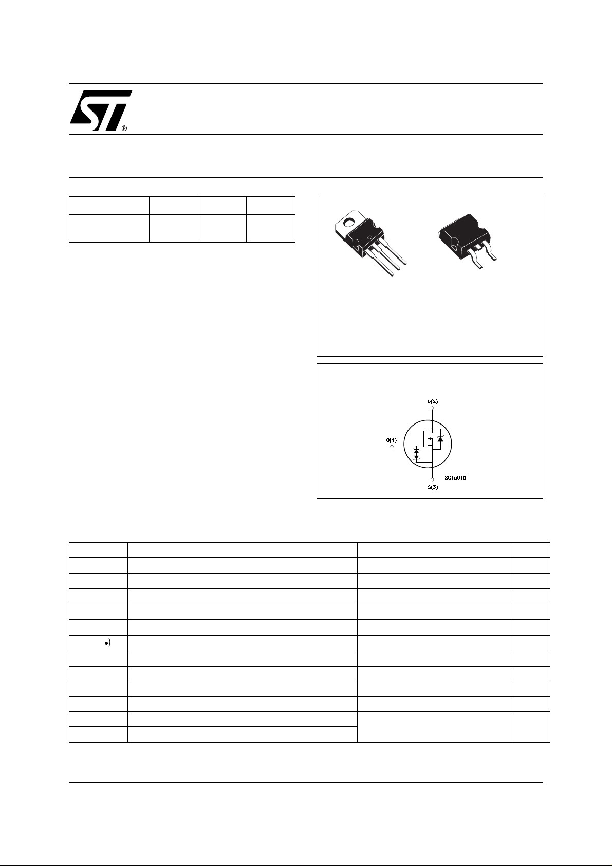
TO-220
3
2
1
1
D2PAK
INTERNAL SCHEMATIC DIAGRAM
3
ABSOLUTE MAXIMUM RATINGS
Symbol Parameter Value Unit
V
DS
V
DGR
V
GS
I
D
I
D
I
DM
P
TOT
V
ESD(G-S)
dv/dt (1) Peak Diode Recovery voltage slope 5 V/ns
T
stg
T
j
(•)Pu l se width limited by safe operating area
Drain-source Voltage (VGS = 0)
Drain-gate Voltage (RGS = 20 kΩ)
250 V
250 V
Gate- source Voltage ± 20 V
Drain Current (continuos) at TC = 25°C
Drain Current (continuos) at TC = 100°C
(l)
Drain Current (pulsed) 88 A
Total Dissipation at TC = 25°C
22 A
13.9 A
135 W
Derating Factor 1.07 W/°C
Gate source ESD(HBM-C=100pF, R=1.5KΩ) 2500 V
Storage Temperature
Max. Operating Junction Temperature
(1) ISD ≤22A, di/dt ≤200A/µs, VDD ≤ V
–55 to 150 °C
, Tj ≤ T
(BR)DSS
JMAX.
1/10January 2002
STP22NS25Z / STB22NS25Z
THERMA L D ATA
Rthj-case Thermal Resistance Junction-case Max 0.93 °C/W
Rthj-amb Thermal Resistance Junction-ambient Max 62.5 °C/W
T
l
AVALANCHE CHARACTERISTICS
Symbol Parameter Max Value Unit
I
AR
E
AS
ELECTRICAL CHARACTERISTICS (TCASE = 25 °C UNLESS OTHERWISE SPECIFIED)
OFF
Symbol Parameter Test Conditions Min. Typ. Max. Unit
V
(BR)DSS
I
DSS
I
GSS
Maximum Lead Temperature For Soldering Purpose 300 °C
Avalanche Current, Repetitive or Not-Repetitive
(pulse width limited by T
max)
j
Single Pulse Avalanche Energy
(starting T
Drain-source
= 25 °C, ID = IAR, VDD = 50 V, Rg = 47 Ohm)
j
ID = 250 µA, VGS = 0 250 V
22 A
350 mJ
Breakdown Voltage
= Max Rating
Zero Gate Voltage
Drain Current (V
GS
Gate-body Leakage
Current (V
DS
= 0)
= 0)
V
DS
VDS = Max Rating, TC = 125 °C
V
= ±18V ±10 µA
GS
10 µA
100 µA
ON
(1)
Symbol Parameter Test Conditions Min. Typ. Max. Unit
V
GS(th)
R
DS(on)
Gate Threshold Voltage
Static Drain-source On
V
= VGS, ID = 250µA
DS
VGS = 10V, ID = 11 A
234V
0.13 0.15 Ω
Resistance
DYNAMIC
Symbol Parameter Test Conditions Min. Typ. Max. Unit
(1) Forward Transconductance VDS > I
g
fs
C
iss
C
oss
C
rss
Input Capacitance
Output Capacitance 340 pF
Reverse Transfer
Capacitance
I
D
V
=11A
DS
D(on)
x R
DS(on)max,
= 25V, f = 1 MHz, VGS = 0
22 S
2400 pF
120 pF
2/10

STP22NS25Z / STB22NS25Z
ELECTRICAL CHARACTERISTICS (CONTINUED)
SWITCHING ON
Symbol Parameter Test Conditions Min. Typ. Max. Unit
V
t
d(on)
Q
Q
Q
t
r
g
gs
gd
Turn-on Delay Time
Rise Time 30 ns
Total Gate Charge
Gate-Source Charge 11 nC
Gate-Drain Charge 40 nC
SWITCHING OFF
Symbol Parameter Test Conditions Min. Typ. Max. Unit
t
d(Voff)
t
t
r(Voff)
t
t
f
f
c
Turn-off- Delay Time
Fall Time
Off-voltage Rise Time
Fall Time
Cross-over Time
SOURCE DRAIN DIODE
Symbol Parameter Test Conditions Min. Typ. Max. Unit
I
SD
I
SDM
VSD (1)
t
rr
Q
rr
I
RRM
Source-drain Current 22 A
(2)
Source-drain Current (pulsed) 88 A
Forward On Voltage
Reverse Recovery Time
Reverse Recovery Charge 3065 nC
Reverse Recovery Current 21 A
= 125 V, ID = 11 A
DD
RG= 4.7Ω VGS = 10 V
(see test circuit, Figure 3)
V
= 200V, ID = 20 A,
DD
VGS = 10V
VDD = 125V, ID = 11 A,
RG=4.7Ω, V
GS
= 10V
(see test circuit, Figure 3)
V
= 200V, ID = 22 A,
clamp
R
=4.7Ω, V
G
GS
= 10V
(see test circuit, Figure 5)
ISD = 22 A, VGS = 0
I
= 22 A, di/dt = 100A/µs
SD
VDD = 50V, Tj = 150°C
(see test circuit, Figure 5)
20 ns
108 151 nC
100
78
37
65
110
1.6 V
292 ns
ns
ns
ns
ns
ns
GATE-SOURCE ZENER DIODE
Symbol Parameter Test Conditions Min. Typ. Max. Unit
BV
GSO
Gate-Source Breakdown
Igs=± 500µA (Open Drain) 20 V
Voltage
Note: 1. Pulsed: Pu l se duration = 300 µs, duty c yc l e 1.5 %.
2. Pulse width li mited by safe operating ar ea.
PROTECTION FEATURES OF GATE-TO-SOURCE ZENER DIODES
The built-in back-to-back Zener diodes have specif ically been designed to enhanc e not only t he dev ice’s
ESD capability, but also to make them safely absorb possible voltage transients that may occasionally be
applied from gate to souce. In this respect the Zener voltage is appropriate to achieve an efficient and costeffective intervention to protect the device’s integrity. These integrated Zener diodes thus avoid the usage
of external components.
3/10
 Loading...