

SGS Thomson Microelectronics STP22NM60, STP22NM60FP, STB22NM60, STB22NM60-1 Datasheet
1/11
ADVANCED DATA
June 2003
STP22NM60 - STF22NM60
STB22NM60 - STB22NM60-1 - STW22NM60
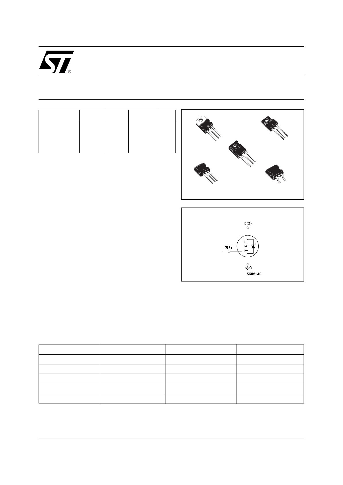
N-CHANNEL 600V - 0.19 Ω - 22A TO-220/FP/D2PAK/I2PAK/TO-247
MDmesh™Power MOSFET
1
2
3
1
3
1
2
3
TO-220FP
I
2
PAK
D
2
PAK
1
2
3
1
2
3
TO-220
TO-247
■ TYPICAL R
DS
(on) = 0.19Ω
■ HIGH dv/dt AND AVALANCHE CAPABILITIES
■ 100% AV ALANCHE TESTED
■ LOW INPUT CAPACITANCE AND GATE CHARGE
■ LOW GATE INPUT RESISTANCE
DESCRIPTION
This improved version of MDmesh™ which is based
on Multiple Drain proc ess represents the new benchmark in high voltage MOSFETs. The resulting product
exhibits ev en lower on-resistance, impressively high
dv/dt and excellent avalanche characteristics. The
adoption of the Company’s proprietary strip technique
yields overall performances that are significantlybetter
than t hat of simi lar compet it ion’s products.
APPLICATIONS
The MDmesh™ family is very suitable for increasing
power density of high voltage converters allowing system miniaturization and higher efficiencies.
ORDERING INFORMATION
TYPE V
DSS
R
DS(on)Rds(on)*QgID
STP22NM60
STF22NM60
STB22NM60
STB22NM60-1
STW22NM60
600 V
600 V
600 V
600 V
600 V
< 0.25 Ω
< 0.25 Ω
< 0.25 Ω
< 0.25 Ω
< 0.25 Ω
7.6 Ω*nC
7.6 Ω*nC
7.6 Ω*nC
7.6 Ω*nC
7.6 Ω*nC
22 A
22 A
22 A
22 A
22 A
SALES TYPE MARKING PACKAGE PACKAGING
STP22NM60 P22NM60 TO-220 TUBE
STF22NM60 F22NM60 TO-220FP TUBE
STB22NM60
B22NM60T4 D
²PAK TAPE & REEL
STB22NM60-1
B22NM60-1 I
²PAK TUBE
STW22NM60 W22NM60 TO-247 TUBE
I
NTERNAL SCHEMATIC DIAGRAM
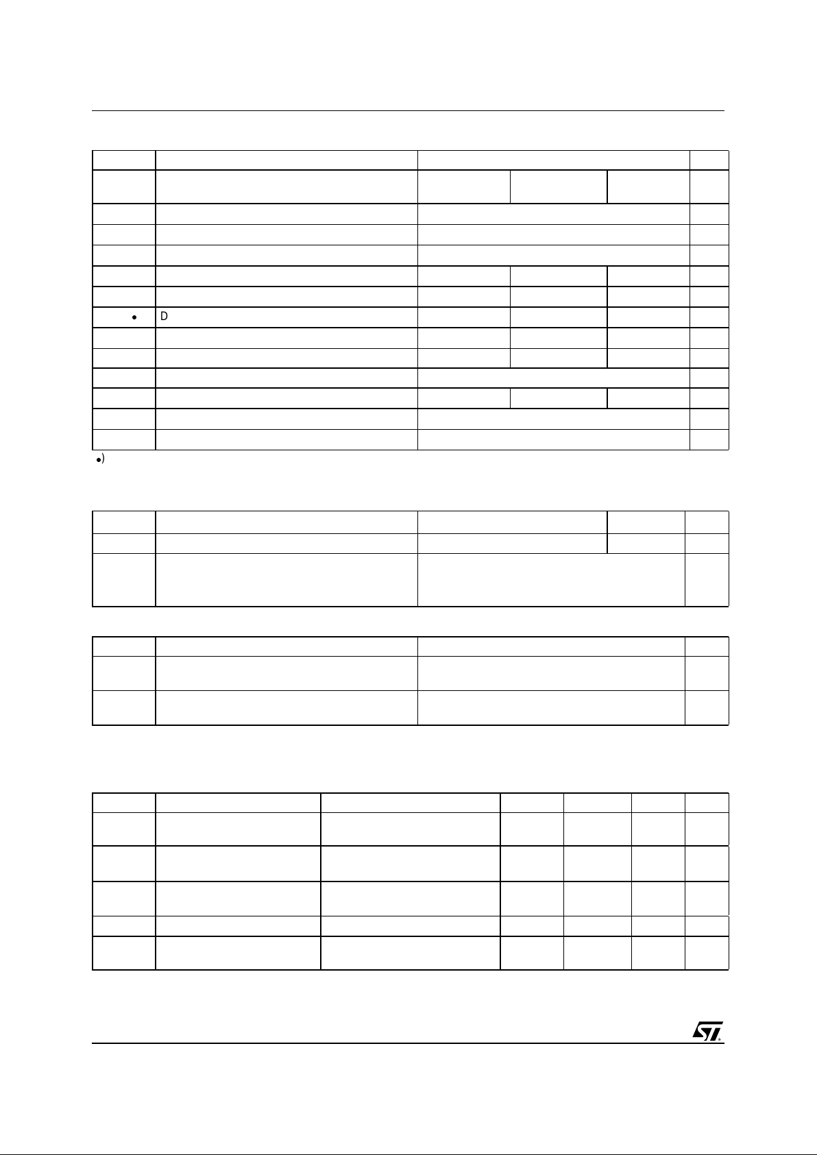
STP22NM60 / STF22NM60 / ST B 22NM6 0 / STB22NM60-1 - STW22NM60
2/11
ABSOLUTE M AXIMUM RA TINGS
() Pulse width limited by safe operating area; (*)Limited only by maximum temperature allowed
(1) I
SD
≤22A, di/dt ≤400A/µs, VDD≤ V
(BR)DSS,Tj≤TJMAX.
THERMAL DATA
AVALANCHE CHARACTERISTICS
ELECTRICAL CHARACT ERISTICS (T
CASE
= 25 °C UNLESS OTHERWISE SPECIFIED)
ON/OFF
Symbol Parameter Value Unit
STP22NM60
STB22NM60/1
STF22NM60 STW22NM60
V
DS
Drain-source Voltage (VGS=0)
600 V
V
DGR
Drain-gate Voltage (RGS=20kΩ)
600 V
V
GS
Gate- source Voltage ±30 V
I
D
Drain Current (continuous) at TC= 25°C
22 22 (*) 22 A
I
D
Drain Current (continuous) at TC= 100°C
12.6 12.6 (*) 12.6 A
I
DM
()
Drain Current (pulsed) 80 80(*) 80 A
P
TOT
Total Dissipation at TC= 25°C
192 45 210 W
Derating Factor 1.2 0.36 1.2 W/°C
dv/dt(1) Peak Diode Recovery voltage slope 15 V/ns
V
ISO
Insulation Winthstand Voltage (DC) -- 2500 -- V
T
stg
Storage Temperature –65 to 150 °C
T
j
Max. Operating Junction Temperature 150 °C
TO-220/D
2
PAK/I2PAK/TO-247
TO-220FP
Rthj-case ThermalResistanceJunction-case Max 0.65 2.8 °C/W
Rthj-amb ThermalResistanceJunction-ambient Max 62.5 °C/W
T
l
Maximum Lead Temperature For Soldering
Purpose
300 °C
Symbol Parameter Max Value Unit
I
AR
Avalanche Current, Repetitive or Not-Repetitive
(pulse width limited by T
j
max)
11 A
E
AS
Single Pulse Avalanche Energy
(starting T
j
=25°C,ID=IAR,VDD=50V)
650 mJ
Symbol Parameter Test Conditions Min. Typ. Max. Unit
V
(BR)DSS
Drain-source
Breakdown Voltage
ID= 250 µA, VGS=0 600 V
I
DSS
Zero Gate Voltage
Drain Current (V
GS
=0)
V
DS
= Max Rating
V
DS
= Max Rating, TC=125°C
1
10
µA
µA
I
GSS
Gate-body Leakage
Current (V
DS
=0)
V
GS
= ±30 V ±100 nA
V
GS(th)
Gate Threshold Voltage
V
DS=VGS,ID
= 250 µA
34
5V
R
DS(on)
Static Drain-source On
Resistance
VGS=10V,ID= 11 A 0.19 0.25 Ω
3/11
STP22NM60 / STF22NM60 / STB22NM60 / STB22NM60-1 - STW22NM60
ELECTRICAL CHARACT ERISTICS (CO NTINUE)
DYNAMIC
(1) Pulsed: Pulse duration = 300 µs, duty cycle 1.5 %.
(*) C
oss eq.
is defined as a constant equivalent capacitance giving the same charging time as C
oss
when VDSincreases from 0 to 80% V
DSS
.
SWITCHING ON
SWITCHING OFF
SOURCE DRAIN DIODE
Note: 1. Pulsed: Pulse duration = 300 µs, duty cycle 1.5 %.
2. Pulse width limited by safe operating area.
Symbol Parameter Test Conditions Min. Typ. Max. Unit
g
fs
(1) Forward Transconductance VDS>I
D(on)xRDS(on)max,
ID=11A
TBD S
C
iss
C
oss
C
rss
Input Capacitance
Output Capacitance
Reverse Transfer
Capacitance
V
DS
=25V,f=1MHz,VGS= 0 1590
803
52
pF
pF
pF
C
oss eq.
(2) Equivalent Output
Capacitance
VGS=0V,VDS= 0V to 400V 130 pF
R
g
Gate Input Resistance f=1 MHz Gate DC Bias=0
Test Signal Level=20mV
Open Drain
1.6 Ω
Symbol Parameter Test Conditions Min. Typ. Max. Unit
t
d(on)
t
r
Turn-on Delay Time
Rise Time
VDD=200V,ID=11A
R
G
= 4.7Ω VGS=10V
(see test circuit, Figure 3)
25
20
ns
ns
Q
g
Q
gs
Q
gd
Total Gate Charge
Gate-Source Charge
Gate-Drain Charge
VDD=400V,ID=22A,
VGS=10V
40
11
25
71
nC
nC
nC
Symbol Parameter Test Conditions Min. Typ. Max. Unit
t
r(Voff)
Off-voltage Rise Time
V
DD
= 480 V, ID=22A,
RG=4.7Ω, VGS=10V
(see test circuit, Figure 5)
13 ns
t
f
Fall Time 15 ns
t
c
Cross-over Time 26 ns
Symbol Parameter Test Conditions Min. Typ. Max. Unit
I
SD
Source-drain Current 20 A
I
SDM
(2)
Source-drain Current (pulsed) 80 A
V
SD
(1)
Forward On Voltage
ISD=22A,VGS=0
1.5 V
t
rr
Q
rr
I
rrm
Reverse Recovery Time
Reverse Recovery Charge
Reverse Recovery Current
I
SD
= 22 A, di/dt = 100 A/µs,
VDD=100V,Tj=25°C
(see test circuit, Figure 5)
416
5.6
27
ns
µC
A
t
rr
Q
rr
I
rrm
Reverse Recovery Time
Reverse Recovery Charge
Reverse Recovery Current
I
SD
= 22 A, di/dt = 100 A/µs,
V
DD
=100V,Tj=150°C
(see test circuit, Figure 5)
544
7.3
28
ns
µC
A

STP22NM60 / STF22NM60 / ST B 22NM6 0 / STB22NM60-1 - STW22NM60
4/11
Fig. 5: Test Circuit For Inductive Load Switching
And Diode Recovery Times
Fig. 4: Gate Charge test Circuit
Fig. 2: Unclamped Inductive WaveformFig. 1: Unclamped Inductive Load Test Circuit
Fig. 3: Switching Times Test Circuit For
Resistive Load
 Loading...