

SGS Thomson Microelectronics STP22NE10L Datasheet

STP22NE10L
N - CHANNEL 100V - 0.07 Ω - 22A TO-220
STripFET POWER MOSFET
TYPE V
DSS
R
DS(on)
I
D
ST P22NE10L 100 V < 0.085 Ω 22 A
■ TYPICALR
■ LOW THRESHOLDDRIVE
■ LOGICLEVEL DEVICE
DS(on)
= 0.07 Ω
DESCRIPTION
This Power MOSFET is the latestdevelopmentof
STMicroelectronics unique ”Single Feature
Size” strip-based process. The resulting
transistor shows extremely high packing density
for low on-resistance, rugged avalanche
characteristics and less critical alignment steps
therefore a remarkable manufacturing
reproducibility.
APPLICATIONS
■ HIGHCURRENT, HIGH SPEED SWITCHING
■ SOLENOIDAND RELAY DRIVERS
■ MOTORCONTROL, AUDIOAMPLIFIERS
■ DC-DC& DC-AC CONVERTERS
3
2
1
TO-220
INTERNAL SCHEMATIC DIAGRAM
ABSOLUTE MAXIMUM RATINGS
Symbol Parameter Value Uni t
V
V
V
I
DM
P
E
AS
T
(•) Pulse width limitedby safe operating area (1) starting Tj
November 1999
Dra in- sour c e Volta ge (VGS= 0) 100 V
DS
Drain- gate Voltage (RGS=20kΩ) 100 V
DGR
Gate-s ource Voltage ± 20 V
GS
Dra in Cu rr ent (conti nuous) at Tc=25oC22A
I
D
Dra in Cu rr ent (conti nuous) at Tc= 100oC14A
I
D
(
Dra in Cu rr ent (pulsed) 88 A
•)
Tot al Dissipatio n at Tc=25oC90W
tot
Der ati ng Fa c t or 0.6 W/
(1) Single Pu lse Avalanche Ener gy 250 mJ
St orage Tempera t ure -65 to 175
stg
Max. Operating Jun ct ion Temperatur e 175
T
j
=25oC,ID=22A , VDD= 50V
o
C
o
C
o
C
1/8

STP22NE10L
THERMAL DATA
R
thj-case
R
thj-amb
T
Ther mal Resistanc e Junct ion-case Max
Ther mal Resistanc e Junct ion-ambie nt Max
Maximum Lead Tempe rat ur e F or S o lder ing P urpose
l
1.67
62.5
300
o
C/W
o
C/W
o
C
ELECTRICAL CHARACTERISTICS
=25oC unless otherwisespecified)
(T
case
OFF
Symbol Parameter Test Condit ions Min. Typ. Max. Unit
V
(BR)DSS
Drain-source
ID=250µAVGS= 0 100 V
Break dow n Vo lt age
I
I
ON (∗
DSS
GSS
Zero Gate Voltage
Drain Curre nt (V
Gat e- bod y Leakag e
Current (V
)
DS
=0)
GS
=0)
V
=MaxRating
DS
=MaxRating Tc=125oC
V
DS
V
= ± 20 V ± 100 nA
GS
1
10
Symbol Parameter Test Condit ions Min. Typ. Max. Unit
V
GS(th)
R
DS(on)
I
D(on)
Gate Threshold Voltage VDS=VGSID= 250 µA11.62.5V
Sta t ic Drain-s our c e On
Resistance
On State Drain Current VDS>I
VGS=10V ID=15A
V
=5V ID=15A
GS
D(on)xRDS(on)max
0.07
0.085
0.085
0.1
22 A
VGS=10V
DYNAMIC
Symbol Parameter Test Condit ions Min. Typ. Max. Unit
g
(∗)Forward
fs
Tr ansc on duc tance
C
C
C
Input Capaci t ance
iss
Out put Capac itance
oss
Reverse Transfer
rss
Capacit a nc e
VDS>I
D(on)xRDS(on)maxID
=15 A 19 S
VDS=25V f=1MHz VGS= 0 1750
165
45
µA
µ
Ω
Ω
pF
pF
pF
A
2/8
STP22NE10L
ELECTRICAL CHARACTERISTICS
(continued)
SWITCHINGON
Symbol Parameter Test Condit ions Min. Typ. Max. Unit
t
d(on)
Tur n-on Delay Tim e
Rise Time
t
r
VDD=50V ID=8A
R
=4.7
G
Ω
VGS=4.5V
40
80
(Resis t iv e Load, see fig. 3 )
Q
Q
Q
Tot al Gate Charge
g
Gat e- Source Charge
gs
Gate-Drain Charge
gd
VDD=80V ID=16A VGS=10V 24
55
11
31 nC
SWITCHINGOFF
Symbol Parameter Test Condit ions Min. Typ. Max. Unit
t
d(off)
Tur n-of f Dela y Tim e
t
Fall T ime
f
VDD=50V ID=8A
=4.7 Ω VGS=4.5V
R
G
45
12
(Resis t iv e Load, see fig. 3 )
t
d(off)
Off-voltage Rise Time
t
Fall T ime
f
t
Cross-over Time
c
Vclamp = 80 V ID=16A
=4.7 Ω VGS=4.5V
R
G
(Indu ct iv e Load, see fig. 5)
12
17
35
SOURCEDRAIN DIODE
Symbol Parameter Test Condit ions Min. Typ. Max. Unit
I
V
I
SDM
SD
Q
I
RRM
SD
t
Source-drain Current
(•)
Source-drain Current
22
88
(pulsed)
(∗)ForwardOnVoltage ISD=16A VGS=0 1.5 V
Reverse Recovery
rr
Time
Reverse Recovery
rr
ISD= 16 A di/dt = 100 A/µs
=40V Tj=150oC
V
DD
(see test circuit, fig. 5)
100
300
Charge
Reverse Recovery
6
Current
ns
ns
nC
nC
ns
ns
ns
ns
ns
A
A
ns
nC
A
(∗) Pulsed: Pulse duration = 300 µs, duty cycle 1.5 %
(•) Pulse width limited by safe operating area
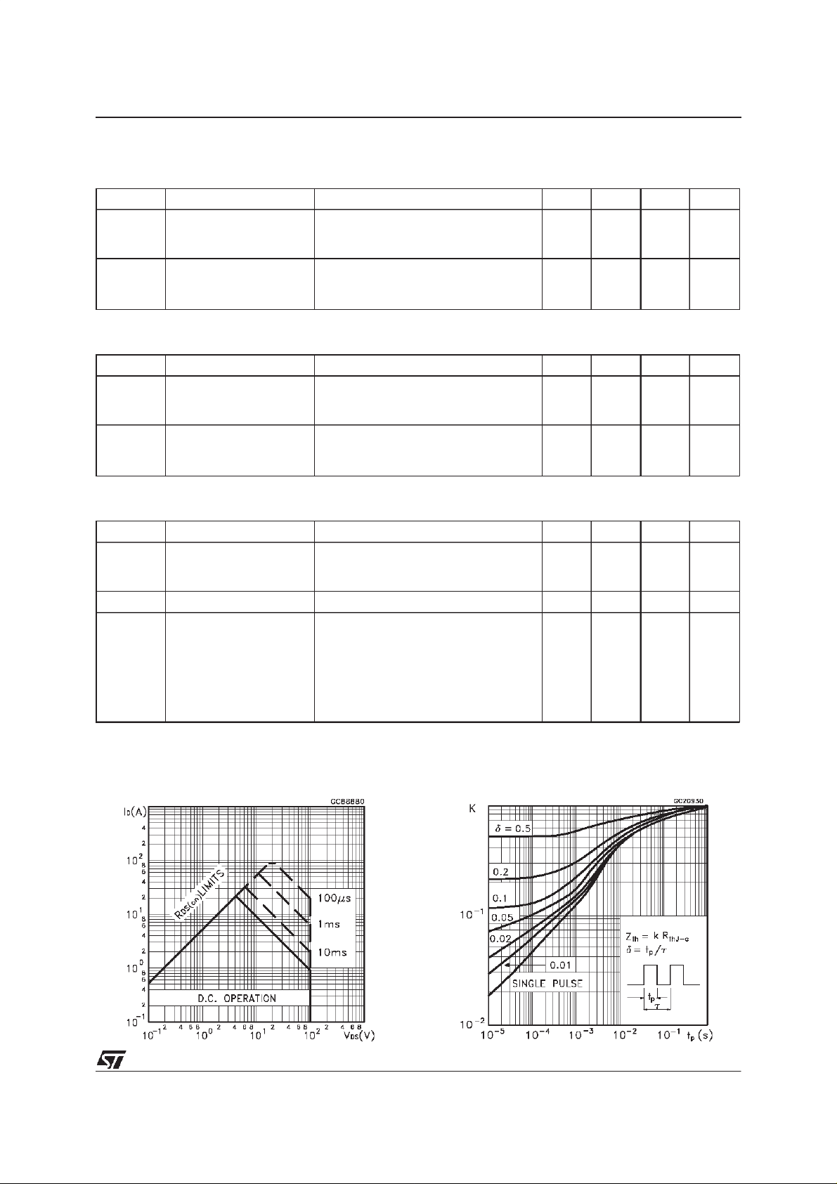
SafeOperating Area ThermalImpedance
3/8
 Loading...