

SGS Thomson Microelectronics STP20NE10 Datasheet
STP20NE10
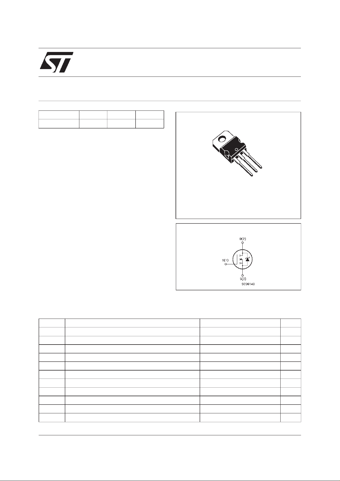
N - CHANNEL 100V - 0.07Ω - 20A - TO-220
STripFET MOSFET
TYPE V
DSS
R
DS(on)
I
D
STP20 NE 1 0 100 V < 0. 1 Ω 20 A
■ TYPICALR
■ EXCEPTIONALdv/dt CAPABILITY
■ 100% AVALANCHETESTED
■ APPLICATIONORIENTED
DS(on)
=0.07 Ω
CHARACTERIZATION
DESCRIPTION
This Power MOSFET is thelatestdevelopment of
SGS-THOMSON unique ”Single Feature Size”
strip-based process.The resulting transistor
shows extremely high packing density for low onresistance, rugged avalanche characteristics and
less critical alignment steps therefore a remarkable manufacturingreproducibility.
APPLICATIONS
■ SOLENOIDANDRELAY DRIVERS
■ MOTORCONTROL, AUDIOAMPLIFIERS
■ DC-DCCONVERTERS
■ AUTOMOTIVE ENVIRONMENT
3
2
1
TO-220
INTERNAL SCHEMATIC DIAGRAM
ABSOLUTE MAXIMUM RATINGS
Symb o l Para meter Value Uni t
V
V
V
I
DM
P
dv/ dt (
T
(•) Pulse width limitedby safe operating area (1)ISD≤ 20 A,di/dt ≤ 300A/µs, VDD≤ V
July 1998
Drain-source Volt age (VGS=0) 100 V
DS
DGR Drain- gate Voltage (R
Gat e- source Voltage ± 20 V
GS
I
Drain C ur rent (continuous) at Tc=25oC20A
D
I
Drain C ur rent (continuous) at Tc=100oC14A
D
=20kΩ)
GS
100 V
(•) Dra in Current (pulsed) 80 A
Tot al Dis sipation at Tc=25oC90W
tot
Derating Factor 0.6 W/
1) Peak Diode Recover y v o lt age slope 7 V/ns
Sto rage T em pe r ature -65 to 17 5
stg
T
Max. O perating J u nc tion Temperat u r e 175
j
(BR)DSS,Tj≤TJMAX
o
C
o
C
o
C
1/8
STP20NE10
THERMAL DATA
R
thj-case
Rthj-amb
R
thc-sin k
T
AVALANCHE CHARACTERISTICS
Symbol Para met e r Max Va lu e Uni t
I
AR
E
Ther mal Resist ance Junction- ca s e Max
Ther mal Resist ance Junction- ambient Max
Ther mal Resist ance Case-sink Typ
Maximum Lead Te mperat u re For Soldering P ur p os e
l
Avalanche C ur re nt , R epetiti ve or Not -Repetit ive
(pulse w idth limited b y T
Single Pulse Avalanche Energy
AS
(starting T
=25oC, ID=IAR,VDD=30V)
j
max, δ <1%)
j
1.67
62.5
0.5
300
20 A
170 mJ
o
C/W
oC/W
o
C/W
o
C
ELECTRICAL CHARACTERISTICS (T
=25oC unlessotherwise specified)
case
OFF
Symbol Parameter Te st Cond itions Min. Typ. Max. Unit
V
(BR)DSS
Drain-source
=250µAVGS=0
I
D
100 V
Breakdown V oltage
I
DSS
I
GSS
Zer o G at e Voltage
Drain Current ( V
GS
Gat e-body Leakage
Current (V
DS
=0)
=0)
=MaxRating
V
DS
V
=MaxRating Tc=125
DS
o
C
= ± 20 V
V
GS
1
10
± 100 nA
ON (∗)
Symbol Parameter Te st Cond itions Min. Typ. Max. Unit
V
GS(th )
Gate Threshold
V
DS=VGSID
=250µA
234V
Voltage
R
DS(on)
Stati c Drain-so urce O n
VGS=10V ID= 10 A 0.07 0.1 Ω
Resistance
I
D(on)
On S tate Drain Cu r re nt VDS>I
D(on)xRDS(on)max
20 A
VGS=10V
DYNAMIC
Symbol Parameter Te st Cond itions Min. Typ. Max. Unit
g
(∗)Forward
fs
Tr ansconductance
C
C
C
Input Ca pac i t an c e
iss
Out put Capa c itance
oss
Reverse T ransfer
rss
Capa cit an c e
VDS>I
D(on)xRDS(on)maxID
=10 A 6 S
VDS=25V f=1MHz VGS= 0 1600
180
50
2100
250
70
µA
µA
pF
pF
pF
2/8
STP20NE10
ELECTRICAL CHARACTERISTICS (continued)
SWITCHINGON
Symbol Parameter Te st Cond itions Min. Typ. Max. Unit
t
d(on)
Turn-on Tim e
r
Rise T ime
t
VDD=30V ID=10A
=4.7 Ω VGS=10V
R
G
17
37
(see test circuit, figure 3)
Q
Q
Q
Total Gate Charge
g
Gat e-Sourc e Cha r ge
gs
Gate-Drain Charge
gd
VDD=80V ID=20A VGS=10V 38
10
12
SWITCHINGOFF
Symbol Parameter Te st Cond itions Min. Typ. Max. Unit
t
r(Voff)
t
t
Of f - voltage Ris e Time
Fall Time
f
Cross-over Time
c
VDD=80V ID=20A
=4.7 Ω VGS=10V
R
G
(see test circuit, figure 5)
11
18
32
SOURCE DRAIN DIODE
Symbol Parameter Te st Cond itions Min. Typ. Max. Unit
I
SD
I
SDM
V
SD
t
Q
I
RRM
(∗) Pulsed: Pulse duration =300 µs,duty cycle 1.5 %
(•) Pulse width limited by safe operating area
Source-drain Cu rrent
(•)
Source-drain Cu rrent
(pulsed)
(∗) For ward O n V o lt age ISD=20A VGS=0 1.5 V
Reverse Recovery
rr
Time
Reverse Recovery
rr
= 20 A di/dt = 10 0 A /µ s
I
SD
=30V Tj=150oC
V
DD
(see test circuit, figure 5)
110
440
Charge
Reverse Recovery
8
Current
23
50
50 nC
15
25
44
16
64
ns
ns
nC
nC
ns
ns
ns
A
A
ns
µC
A
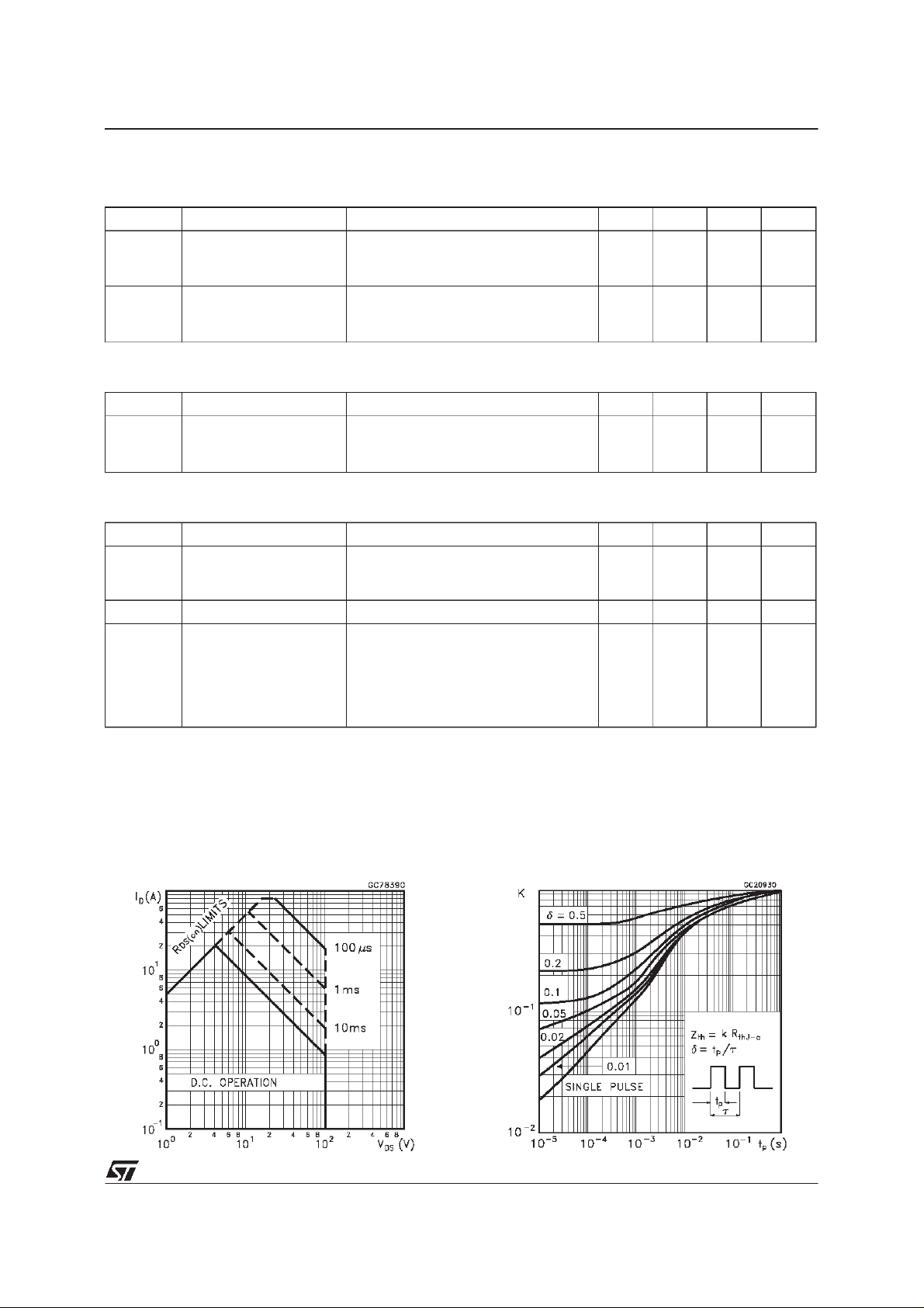
Safe Operating Area ThermalImpedance
3/8
 Loading...