

SGS Thomson Microelectronics STP19NB20FP, STP19NB20 Datasheet
STP19NB20
N - CHANNEL ENHANCEMENT MODE
TYPE V
STP19NB20
ST P19NB20FP
■ TYPICALR
■ EXTREMELYHIGH dv/dtCAPABILITY
■ 100%AVALANCHETESTED
■ VERYLOW INTRINSIC CAPACITANCES
■ GATECHARGE MINIMIZED
DS(on)
DSS
200 V
200 V
= 0.150 Ω
DESCRIPTION
Using the latest high voltage MESH OVERLAY
process, STMicroelectronics has designed an
advanced family of power MOSFETs with
outstanding performances. The new patent
pending strip layout coupled with the Company’s
proprietary edge termination structure, gives the
lowest RDS(on) per area, exceptional avalanche
and dv/dt capabilities and unrivalled gate charge
and switching characteristics.
R
DS(on)
< 0.180 Ω
< 0.180 Ω
I
D
19 A
10 A
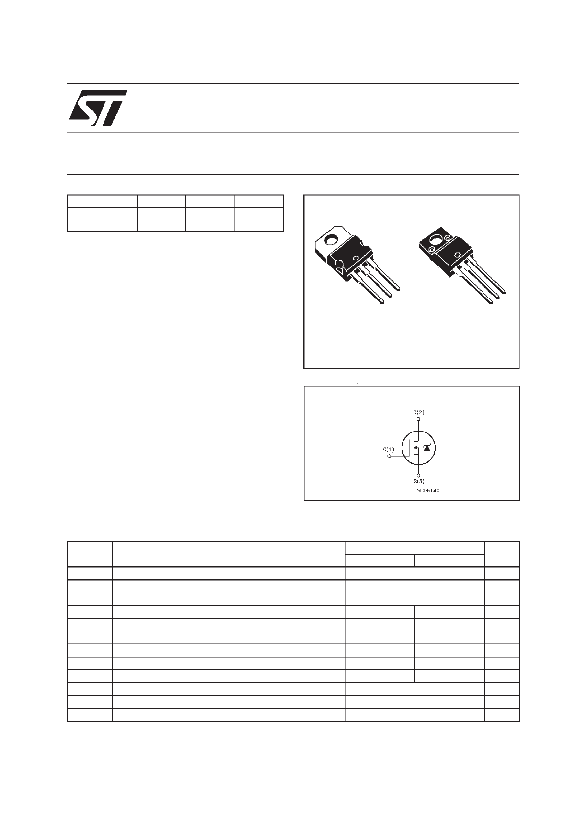
STP19NB20FP
PowerMESH MOSFET
3
2
1
TO-220 TO-220FP
INTERNAL SCHEMATIC DIAGRAM
3
2
1
APPLICATIONS
■ HIGHCURRENT, HIGH SPEED SWITCHING
■ SWITCHMODE POWER SUPPLIES (SMPS)
■ DC-AC CONVERTERS FOR WELDING
EQUIPMENTANDUNINTERRUPTIBLE
POWERSUPPLIESAND MOTOR DRIVE
ABSOLUTE MAXIMUM RATINGS
Symbol Parameter Value Unit
STP 19NB20 ST P19NB20F P
V
V
V
I
DM
P
dv/dt(
V
T
(•) Pulse width limited by safe operating area (1)ISD≤ 19A, di/dt ≤ 300A/µs, VDD≤ V
Dra in- sour c e Volt age (VGS= 0) 200 V
DS
Dra in- gat e Voltage (RGS=20kΩ) 200 V
DGR
Gat e-source Voltage ± 30 V
GS
Dra in Cu rr ent ( c ont inuous) at Tc=25oC1910A
I
D
Dra in Cu rr ent ( c ont inuous) at Tc=100oC126.0A
I
D
(•) D r a in Cu rr ent (pulsed ) 76 76 A
Tot al Dis s ipation at Tc=25oC 125 35 W
tot
Derating Factor 1 0.28 W/
) P eak Diode Rec ov er y volt age sl ope 5.5 5.5 V/ns
1
Ins u lat ion Withs t a nd Volt age (D C) 2000 V
ISO
St orage Temper at ure -65 to 150
stg
Max. Operating Junc t ion Temperat ur e 150
T
j
(BR)DSS
,Tj≤T
JMAX
o
C
o
C
o
C
June 1998
1/9
STP19NB20/FP
THERMAL DATA
TO-220 TO 220FP
R
thj-case
R
thj-amb
R
thc-sink
T
AVALANCHE CHARACTERISTICS
Symbol Parameter Max V alue Unit
I
AR
E
Ther mal Res istance Junct ion-case M a x 1 3.57
Ther mal Res istance Junct ion-ambie nt Max
Ther mal Res istance C as e - sink Typ
Maximum Lead T e m pe rat ur e F or So ldering Purpose
l
Avalanche Current, Repetitive or Not-Repetitive
(pulse width limited by T
Single Pul se Avalanc he E nergy
AS
(starting T
=25oC, ID=IAR,VDD=50V)
j
max)
j
62.5
0.5
300
19 A
580 mJ
o
C/W
o
C/W
o
C/W
o
C
ELECTRICAL CHARACTERISTICS
=25oC unless otherwisespecified)
(T
case
OFF
Symbol Parameter Test Conditions Min. Typ. Max. Unit
V
(BR)DSS
Drain-source
ID=250µAVGS= 0 200 V
Break dow n Vo lt age
I
DSS
I
GSS
Zero Gate Voltage
Drain Curre nt (V
GS
Gat e- bod y Leakag e
Current (V
DS
=0)
=0)
V
=MaxRating
DS
=MaxRating Tc=125oC
V
DS
V
=± 30 V
GS
1
10
100 nA
±
ON(∗)
Symbol Parameter Test Conditions Min. Typ. Max. Unit
V
GS(th)
R
DS(on)
Gate Threshold Voltage VDS=VGSID= 250µA 345V
Sta t ic Drain-s our c e On
VGS=10V ID= 9.5 A 0.150 0.180
Resistance
I
D(on)
On StateDrain Current VDS>I
D(on)xRDS(on)ma x
19 A
VGS=10V
DYNAMIC
Symbol Parameter Test Conditions Min. Typ. Max. Unit
g
(∗)Forward
fs
Tr ansc on duc tance
C
C
C
Input Capaci t ance
iss
Out put Capac itance
oss
Reverse Transfer
rss
Capacit a nc e
VDS>I
D(on)xRDS(on)ma xID
=9.5 A 3 S
VDS=25V f=1MHz VGS= 0 1000
285
45
1350
385
60
µA
µA
Ω
pF
pF
pF
2/9
STP19NB20/FP
ELECTRICAL CHARACTERISTICS
(continued)
SWITCHINGON
Symbol Parameter Test Conditions Min. Typ. Max. Unit
t
d(on)
t
r
Turn-on Time
Rise Time
VDD=100V ID= 9.5 A
R
=4.7
G
Ω
VGS=10V
15
15
20
20
(see test circuit, figure 3)
Q
Q
Q
Tot al Gate C harge
g
Gat e- Source Charge
gs
Gate-Drain Charge
gd
VDD= 160 V ID=19A VGS=10V 29
9.5
13
40 nC
SWITCHINGOFF
Symbol Parameter Test Conditions Min. Typ. Max. Unit
t
r(Voff)
t
t
Off-voltage Ris e Time
Fall T ime
f
Cross-over Time
c
VDD=160V ID=19A
=4.7 Ω VGS=10V
R
G
(see test circuit, figure 5)
10
10
20
15
15
30
SOURCEDRAINDIODE
Symbol Parameter Test Conditions Min. Typ. Max. Unit
I
SD
I
SDM
V
SD
t
Q
I
RRM
(∗) Pulsed:Pulse duration = 300µs, duty cycle 1.5%
(•) Pulse width limited by safeoperating area
Source-drain Current
(•)
Source-drain Current
19
76
(pulsed)
(∗)ForwardOnVoltage ISD=19 A VGS=0 1.5 V
Reverse Recovery
rr
Time
Reverse Recovery
rr
ISD=19 A di/ dt = 100 A/µs
=50V Tj= 150oC
V
DD
(see test circuit, figure 5)
210
1.5
Charge
Reverse Recovery
14.5
Current
ns
ns
nC
nC
ns
ns
ns
A
A
ns
µ
A
C
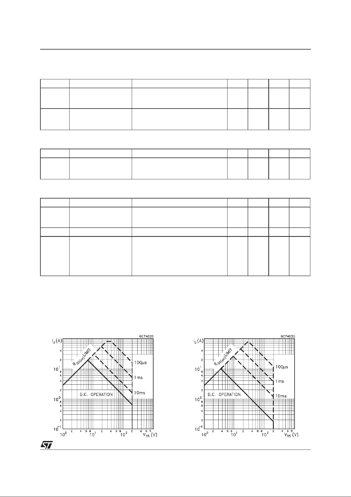
SafeOperating Area for TO-220 SafeOperating Area for TO-220FP
3/9
 Loading...