

SGS Thomson Microelectronics STP16N10L Datasheet
®
STP16N10L
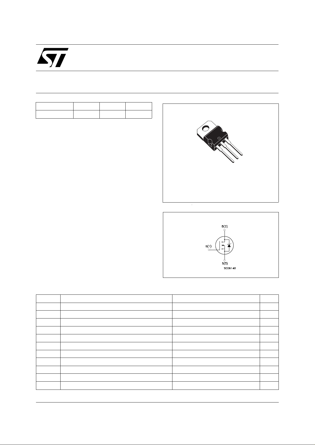
N - CHANNEL 100V - 0.14 Ω - 16A - TO-220
POWER MOS TRANSISTOR
TYPE V
DSS
R
DS(on)
I
D
STP16N10L 100 V < 0.16 Ω 16 A
■
TYPICAL R
■
AVALANCHE RUGG ED TECHNOLO GY
■
100% AVALANCHE TESTED
■
REPETITIVE AVALANCHE DATA AT 100oC
■
HIGH CURRENT CAPABILITY
■
175oC OPERATING TEMPERATURE
■
HIGH dV/dt RUGGEDNESS
■
APPLICATION ORIENTED
DS(on)
= 0.14
Ω
CHARACTERIZATION
APPLICATIONS
■
HIGH CURRENT, HIGH SPEED SWITCH ING
■
POWER MOTOR CONTROL
■
DC-DC & DC-AC CONVERTERS
■
SYNCRONOUS RECTIFICATION
3
2
1
TO-220
INTERNAL SCHEMATIC DIAGRAM
ABSOLUTE MAXIMUM RATINGS
Symbol Parameter Value Unit
V
V
V
I
DM
P
dV/dt(1) Peak Diode Recovery voltage slope 0.6 V/ns
T
March 1999
Drain-source Voltage (VGS = 0) 100 V
DS
Drain- gate Voltage (RGS = 20 kΩ)100V
DGR
Gate-source Voltage ± 15 V
GS
I
Drain Current (continuous) at Tc = 25 oC16A
D
I
Drain Current (continuous) at Tc = 100 oC11A
D
(•) Drain Current (pulsed) 64 A
Total Dissipation at Tc = 25 oC90W
tot
Derating Factor 0.4 W/
Storage Temperature -65 to 175
stg
T
Max. Operating Junction Temperature 175
j
o
C
o
C
o
C
1/5
STP16N10L
THERMAL DATA
R
thj-case
R
thj-amb
R
thc-sink
T
Thermal Resistance Junction-case Max
Thermal Resistance Junction-ambient Max
Thermal Resistance Case-sink Typ
Maximum Lead Temperature For Soldering Purpose
l
AVALANCHE CHARACTERIST ICS
Symbol Parameter Max Value Unit
I
AR
E
Avalanche Current, Repetitive or Not-Repetitive
(pulse width limited by T
Single Pulse Avalanche Energy
AS
(starting T
= 25 oC, ID = IAR, V
j
max)
j
DD
= 50 V)
1.67
62.5
0.5
300
16 A
150 mJ
o
C/W
o
C/W
o
C/W
o
C
ELECTRICAL CHARACTERISTICS
= 25 oC unless otherwise specified)
(T
case
OFF
Symbol Parameter Test Conditions Min. Typ. Max. Unit
V
(BR)DSS
Drain-source
ID = 250 µA V
= 0 100 V
GS
Breakdown Voltage
I
DSS
I
GSS
Zero Gate Voltage
Drain Current (V
GS
Gate-body Leakage
Current (V
DS
= 0)
= 0)
= Max Rating
V
DS
V
= Max Rating Tc = 125 oC
DS
= ± 15 V ± 100 nA
V
GS
1
10
ON (∗)
Symbol Parameter Test Conditions Min. Typ. Max. Unit
V
GS(th)
R
DS(on)
I
D(on)
Gate Threshold Voltage V
Static Drain-source On
Resistance
= VGS ID = 250 µA 1 1.7 2.5 V
DS
VGS = 5V ID = 8 A
V
= 10V ID = 8 A
GS
On State Drain Current VDS > I
V
= 10 V
GS
D(on)
x R
DS(on)max
0.14
0.12
16 A
0.16
0.14
DYNAMIC
Symbol Parameter Test Conditions Min. Typ. Max. Unit
g
(∗) Forward
fs
Transconductance
C
C
C
Input Capacitance
iss
Output Capacitance
oss
Reverse Transfer
rss
Capacitance
VDS > I
V
DS
x R
D(on)
DS(on)max
= 25 V f = 1 MHz V
ID = 8 A 6.5 10 S
50
1100
200
70
= 0 800
GS
150
µA
µA
Ω
Ω
pF
pF
pF
2/5
 Loading...