

SGS Thomson Microelectronics STP14NF10, STP14NF10FP, STB14NF10 Datasheet
STB14NF10
STP14NF10 STP14NF10FP
N-CHANNEL 100V - 0.115 Ω - 15A TO-220/TO-220FP/D2PAK
LOW GATE CHARGE STripFET™ II POWER MOSFET
TYPE
STB14NF10
STP14NF10
STP14NF10FP
■ TYPICAL R
■ EXCEPTIONA L dv/d t CAPABILITY
■ 100% AVALANCHE TESTED
■ APPLICATION ORIENTED
V
DSS
100 V
100 V
100 V
(on) = 0.115 Ω
DS
R
DS(on)
<0.13
<0.13
<0.13
I
D
15 A
Ω
15 A
Ω
10 A
Ω
CHARACTERIZATION
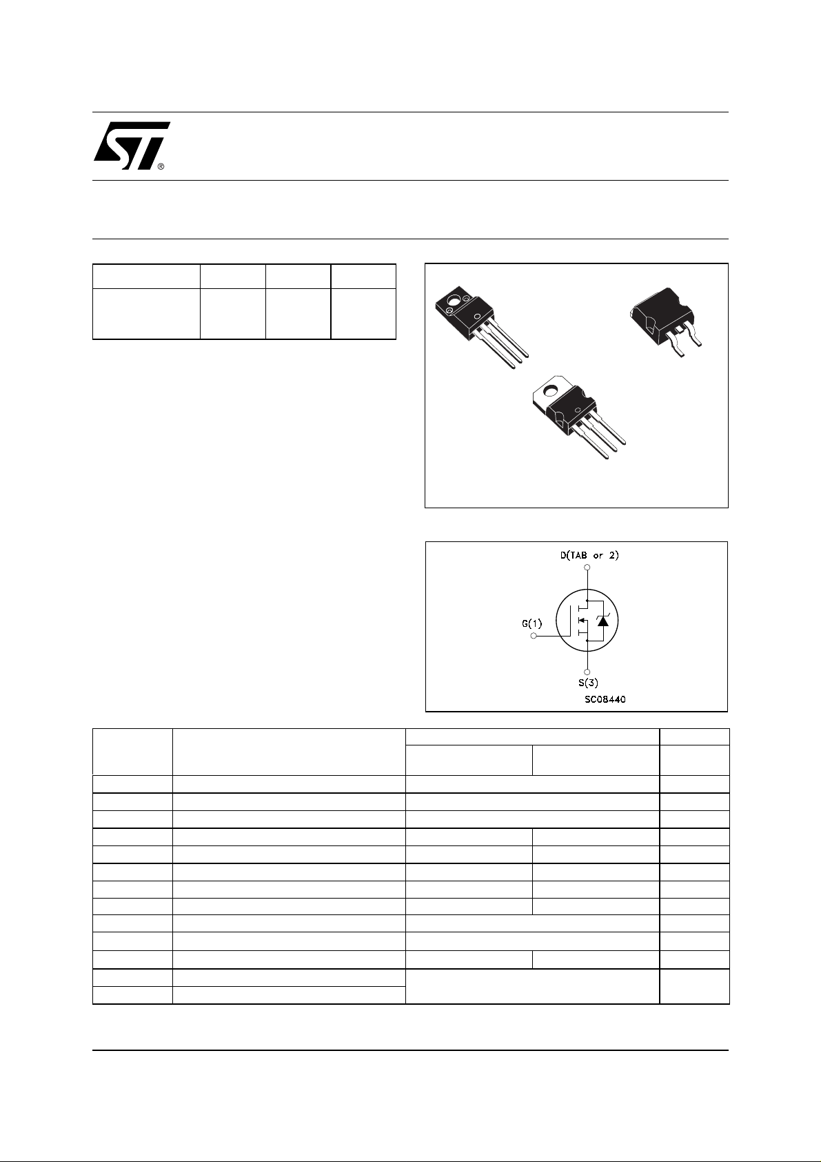
■ SURFACE-MOUNTING D
2
PAK (TO-263)
POWER PACKAG E IN TU BE (NO SU FFIX) OR
IN TAPE & REEL (SUFFIX “T4”)
DESCRIPTION
This MOSFET series realized with STMicroelectronics
unique STripFET™ process has specifically been designed to minimiz e inpu t capa citanc e and gate c harge . It
is therefore su itable as p rima ry sw itch i n ad vanced hig hefficiency, high-frequency isolate d DC-DC c onverters for
T elecom and Computer applications. It is also intended for
any applications with low gate drive requirements.
APPLICATIONS
■ HIGH-EFFICIENCY DC-DC CONVERTERS
■ UPS AND MOTOR CONTROL
3
2
1
TO-220FP
3
2
1
TO-220
INTERNAL SCHEMATIC DIAGRAM
1
D2PAK
TO-263
(Suffix “T4”)
3
ABSOLUTE MAXIMUM RATINGS
Symbol Parameter Value Unit
STB14NF10
STP14NF10
Drain-source Voltage (VGS = 0)
Drain-gate Voltage (RGS = 20 kΩ)
Gate- source Voltage ± 20 V
Drain Current (continuous) at TC = 25°C
Drain Current (continuous) at TC = 100°C
•)
Drain Current (pulsed) 60 40 A
Total Dissipation at TC = 25°C
15 10 A
10 6.3 A
60 25 W
V
I
V
V
DM
P
DS
DGR
GS
I
D
I
D
(
tot
Derating Factor 0.4 0.17 W/°C
(1)
dv/dt
E
AS
V
ISO
T
stg
T
j
(
Pulse width l i mited by safe operating area . (1) ISD ≤14A, di/dt ≤300A/ µ s , VDD ≤ V
•)
.
Peak Diode Recovery voltage slope 9 V/ns
(2)
Single Pulse Avalanche Energy 70 mJ
Insulation Withstand Voltage (DC) ------ 2000 V
Storage Temperature
Operating Junction Temperature
(2) Starting Tj = 25 oC, ID = 15A, VDD= 50V
-55 to 175 °C
STP14NF10FP
100 V
100 V
, Tj ≤ T
(BR)DSS
JMAX
1/11June 2002
STB14NF10 STP14NF10 STP14NF10FP
THERMA L D ATA
D2PAK
TO-220
Rthj-case Thermal Resistance Junction-case Max 2.5 6 °C/W
TO-220FP
Rthj-amb
T
ELECTRICAL CHARACTERISTICS (T
Thermal Resistance Junction-ambient
Maximum Lead Temperature For Soldering Purpose
l
= 25 °C unless otherwise specified)
case
Max 62.5
300
OFF
Symbol Parameter Test Conditions Min. Typ. Max. Unit
I
= 250 µA, VGS = 0
D
V
= Max Rating
DS
V
= Max Rating TC = 125°C
DS
V
= ± 20 V
GS
100 V
1
10
±100 nA
ON
V
(BR)DSS
I
DSS
I
GSS
(*)
Drain-source
Breakdown Voltage
Zero Gate Voltage
Drain Current (V
GS
Gate-body Leakage
Current (V
DS
= 0)
= 0)
Symbol Parameter Test Conditions Min. Typ. Max. Unit
V
GS(th)
R
DS(on)
Gate Threshold Voltage
Static Drain-source On
= VGS I
DS
V
= 10 V ID = 7 A
GS
= 250 µA
D
234V
0.115 0.13
V
Resistance
DYNAMIC
Symbol Parameter Test Conditions Min. Typ. Max. Unit
(*)
g
fs
C
iss
C
oss
C
rss
Forward Transconductance
Input Capacitance
Output Capacitance
Reverse Transfer
Capacitance
V
= 15 V ID=7 A
DS
= 25V, f = 1 MHz, VGS = 0
V
DS
20 S
460
70
30
°C/W
°C
µA
µA
Ω
pF
pF
pF
2/11
STB14NF10 STP14NF10 STP14NF10FP
ELECTRICAL CHARACTERISTICS (continued)
SWITCHING ON
Symbol Parameter Test Conditions Min. Typ. Max. Unit
= 50 V ID = 7 A
t
d(on)
Turn-on Delay Time
t
r
Rise Time
V
DD
R
= 4.7 Ω VGS = 10 V
G
(Resistive Load, Figure 3)
Q
g
Q
gs
Q
gd
Total Gate Charge
Gate-Source Charge
Gate-Drain Charge
= 80 V ID= 12 A VGS= 10V
V
DD
SWITCHING OFF
Symbol Parameter Test Conditions Min. Typ. Max. Unit
= 50 V ID = 7 A
t
d(off)
Turn-off Delay Time
t
f
Fall Time
V
DD
R
= 4.7Ω, V
G
GS
= 10 V
(Resistive Load, Figure 3)
SOURCE DRAIN DIODE
Symbol Parameter Test Conditions Min. Typ. Max. Unit
I
SD
I
SDM
V
SD
t
rr
Q
rr
I
RRM
(*)
Pulsed: P ul se duration = 300 µs, duty cycle 1. 5 %.
(
•)Pulse width limited by saf e operating ar ea.
Source-drain Current
(•)
Source-drain Current (pulsed)
(*)
Forward On Voltage
Reverse Recovery Time
Reverse Recovery Charge
Reverse Recovery Current
I
= 14 A VGS = 0
SD
= 14 A di/dt = 100A/µs
I
SD
V
= 50 V Tj = 150°C
DD
(see test circuit, Figure 5)
16
25
15.5
3.7
4.7
32
8
90
230
5
21 nC
15
60
1.5 V
ns
ns
nC
nC
ns
ns
A
A
ns
nC
A
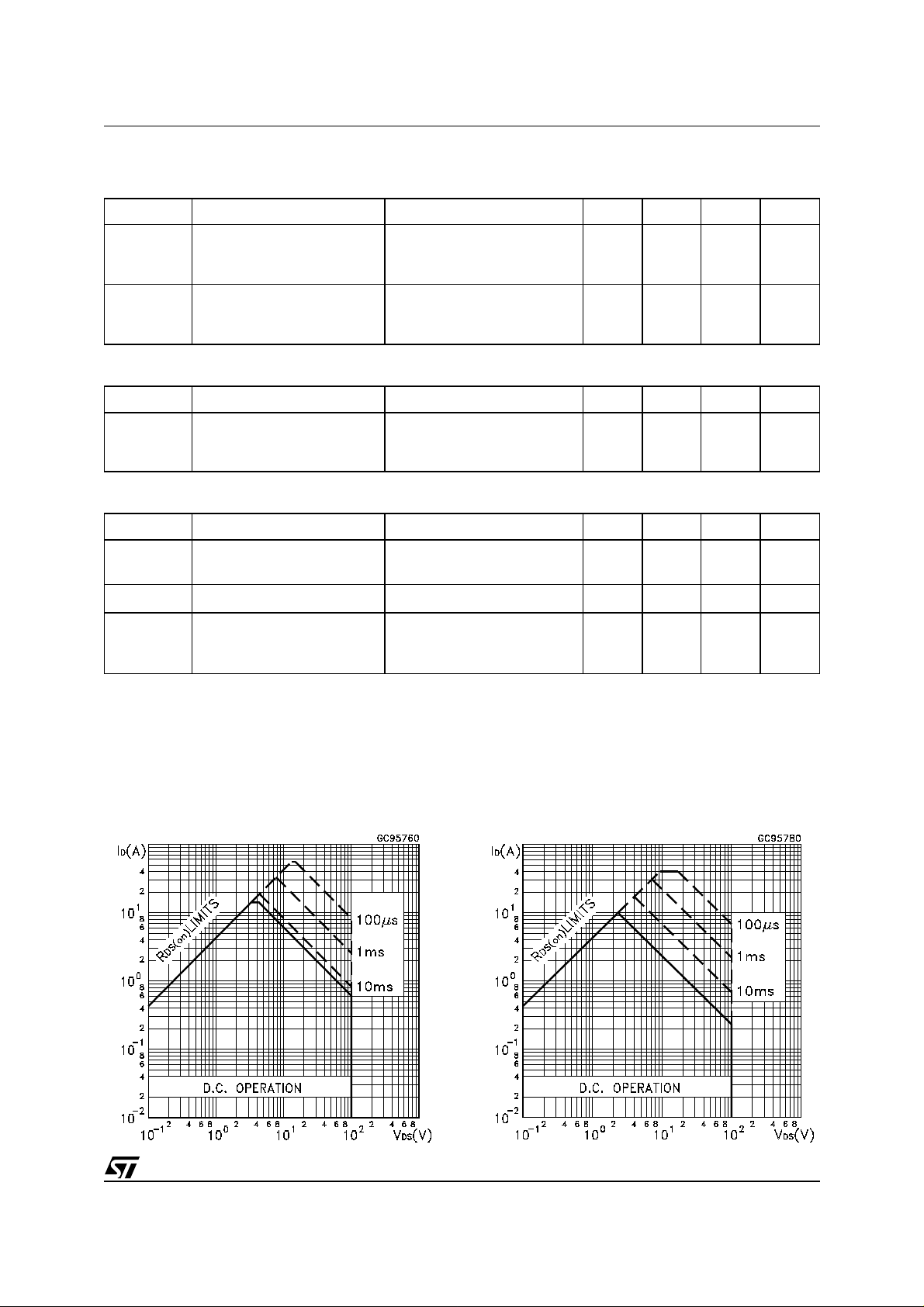
Safe Operating Area for TO-220FPSafe Operating Area for TO-220
3/11
STB14NF10 STP14NF10 STP14NF10FP
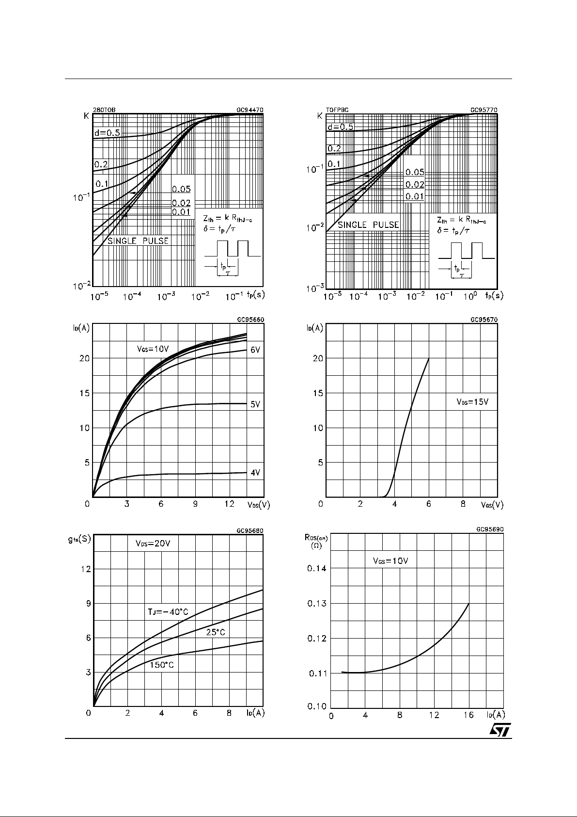
Thermal Impedance Thermal Impedance for TO-220FP
Output Characteristics Transfer Characteristics
Transconductance Static Drain-source On Resistance
4/11
 Loading...